• Photonics Research
  • Vol. 10, Issue 12, 2778 (2022)
Li Chen1、2、†,*, Jie Sun1、†, Wei Guo1、2, Jason Hoo3, Wei Lin4, Hangyang Chen4, Houqiang Xu1、5, Long Yan3, Shiping Guo3, Junyong Kang4, and Jichun Ye1、2、6
Author Affiliations
  • 1Zhejiang Engineering Research Center for Energy Optoelectronic Materials and Devices, Ningbo Institute of Materials Technology and Engineering, Chinese Academy of Sciences, Ningbo 315201, China
  • 2Yongjiang Laboratory, Ningbo 315201, China
  • 3Advanced Micro-Fabrication Equipment Inc., Shanghai 201201, China
  • 4Department of Physics, Xiamen University, Xiamen 361005, China
  • 5University of Chinese Academy of Sciences, Beijing 100049, China
  • 6e-mail:
  • show less
    DOI: 10.1364/PRJ.459897 Cite this Article Set citation alerts
    Li Chen, Jie Sun, Wei Guo, Jason Hoo, Wei Lin, Hangyang Chen, Houqiang Xu, Long Yan, Shiping Guo, Junyong Kang, Jichun Ye. Multi-step in situ interface modification method for emission enhancement in semipolar deep-ultraviolet light emitting diodes[J]. Photonics Research, 2022, 10(12): 2778 Copy Citation Text show less
    (a) Schematic structure and (b) wafer temperature and the corresponding surface reflectivity of multi-layer in situ treated AlN. (c) Mirror-like and crack-free in situ treated AlN surface. (d) AFM images of in situ and ex situ treated AlN. (e) Pole figure of AlN (112¯2), (0002), and sapphire (022¯4) plane diffractions. (f) FWHM of XRC diffraction of AlN templates as a function of azimuth angles.
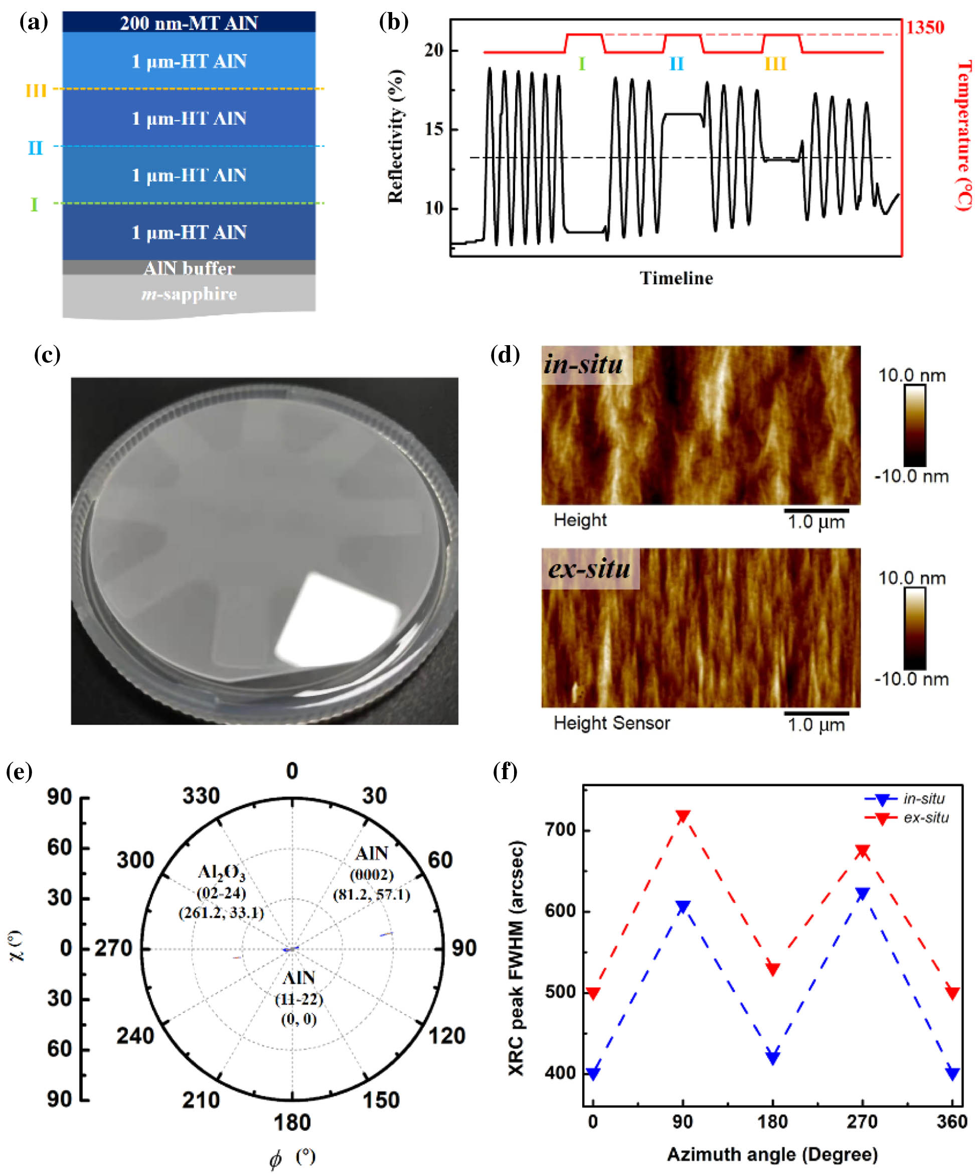
    Fig. 1. (a) Schematic structure and (b) wafer temperature and the corresponding surface reflectivity of multi-layer in situ treated AlN. (c) Mirror-like and crack-free in situ treated AlN surface. (d) AFM images of in situ and ex situ treated AlN. (e) Pole figure of AlN (112¯2), (0002), and sapphire (022¯4) plane diffractions. (f) FWHM of XRC diffraction of AlN templates as a function of azimuth angles.
    (a) ADF images of in situ treated AlN template taken along [11¯00] and [112¯3] zone axes. (b) Optical transmission spectra and (c) Raman spectra of in situ and ex situ treated AlN templates.
    Fig. 2. (a) ADF images of in situ treated AlN template taken along [11¯00] and [112¯3] zone axes. (b) Optical transmission spectra and (c) Raman spectra of in situ and ex situ treated AlN templates.
    (112¯2) symmetric RSM of semipolar DUV LEDs grown on in situ and ex situ treated AlN templates measured along (a) ⟨112¯3⟩ and (b) ⟨11¯00⟩ directions. (c) (112¯4) asymmetric RSM of semipolar DUV LEDs on in situ and ex situ treated AlN templates. (d) Adjusted (112¯4) peak positions of asymmetric RSM according to the different tilt angle of each layer.
    Fig. 3. (112¯2) symmetric RSM of semipolar DUV LEDs grown on in situ and ex situ treated AlN templates measured along (a) 112¯3 and (b) 11¯00 directions. (c) (112¯4) asymmetric RSM of semipolar DUV LEDs on in situ and ex situ treated AlN templates. (d) Adjusted (112¯4) peak positions of asymmetric RSM according to the different tilt angle of each layer.
    Overall and enlarged ADF images of DUV LEDs on the in situ treated AlN template along (a) [11¯00] and (b) [112¯3] zone axes. ADF images of DUV LEDs on the ex situ annealed AlN template and the corresponding enlarged images of defects around the interface along (c) [11¯00] and (d) [112¯3] zone axes. (e) Schematic of the transformation of three types of defects, DI, DII, and DIII, in AlN and AlGaN layers. (f) PL spectra of DUV LEDs on different AlN templates.
    Fig. 4. Overall and enlarged ADF images of DUV LEDs on the in situ treated AlN template along (a) [11¯00] and (b) [112¯3] zone axes. ADF images of DUV LEDs on the ex situ annealed AlN template and the corresponding enlarged images of defects around the interface along (c) [11¯00] and (d) [112¯3] zone axes. (e) Schematic of the transformation of three types of defects, DI, DII, and DIII, in AlN and AlGaN layers. (f) PL spectra of DUV LEDs on different AlN templates.
    High-resolution TEM images of (a) as-grown and (b) HTA-treated AlN films. (c) Ideal AlN and (d), (e) distorted AlN after high-temperature annealing. (f) Radial distribution function of N atoms around an Al atom by high-temperature annealing.
    Fig. 5. High-resolution TEM images of (a) as-grown and (b) HTA-treated AlN films. (c) Ideal AlN and (d), (e) distorted AlN after high-temperature annealing. (f) Radial distribution function of N atoms around an Al atom by high-temperature annealing.
    Li Chen, Jie Sun, Wei Guo, Jason Hoo, Wei Lin, Hangyang Chen, Houqiang Xu, Long Yan, Shiping Guo, Junyong Kang, Jichun Ye. Multi-step in situ interface modification method for emission enhancement in semipolar deep-ultraviolet light emitting diodes[J]. Photonics Research, 2022, 10(12): 2778
    Download Citation