Li Chen1,2,†,*, Jie Sun1,†, Wei Guo1,2..., Jason Hoo3, Wei Lin4, Hangyang Chen4, Houqiang Xu1,5, Long Yan3, Shiping Guo3, Junyong Kang4 and Jichun Ye1,2,6|Show fewer author(s)
1Zhejiang Engineering Research Center for Energy Optoelectronic Materials and Devices, Ningbo Institute of Materials Technology and Engineering, Chinese Academy of Sciences, Ningbo 315201, China
2Yongjiang Laboratory, Ningbo 315201, China
3Advanced Micro-Fabrication Equipment Inc., Shanghai 201201, China
4Department of Physics, Xiamen University, Xiamen 361005, China
5University of Chinese Academy of Sciences, Beijing 100049, China
Li Chen, Jie Sun, Wei Guo, Jason Hoo, Wei Lin, Hangyang Chen, Houqiang Xu, Long Yan, Shiping Guo, Junyong Kang, Jichun Ye, "Multi-step in situ interface modification method for emission enhancement in semipolar deep-ultraviolet light emitting diodes," Photonics Res. 10, 2778 (2022)
Copy Citation Text
Semipolar III-nitrides have attracted increasing attention in applications of optoelectronic devices due to the much reduced polarization field. A high-quality semipolar AlN template is the building block of semipolar AlGaN-based deep-ultraviolet light emitting diodes (DUV LEDs), and thus deserves special attention. In this work, a multi-step in situ interface modification technique is developed for the first time, to our knowledge, to achieve high-quality semipolar AlN templates. The stacking faults were efficiently blocked due to the modification of atomic configurations at the related interfaces. Coherently regrown AlGaN layers were obtained on the in situ treated AlN template, and stacking faults were eliminated in the post-grown AlGaN layers. The strains between AlGaN layers were relaxed through a dislocation glide in the basal plane and misfit dislocations at the heterointerfaces. In contrast, high-temperature ex situ annealing shows great improvement in defect annihilation, yet suffers from severe lattice distortion with strong compressive strain in the AlN template, which is unfavorable to the post-grown AlGaN layers. The strong enhancement of luminous intensity is achieved in in situ treated AlGaN DUV LEDs. The in situ interface modification technique proposed in this work is proven to be an efficient method for the preparation of high-quality semipolar AlN, showing great potential towards the realization of high-efficiency optoelectronic devices.
1. INTRODUCTION
AlGaN-based deep-ultraviolet (DUV) light emitting diodes (LEDs) have wide application prospects in water purification, sterilization, bio-chemical sensing, non-line-of-sight communication, etc. [1]. Although much progress has been made with technological breakthroughs/innovations, the relatively low quantum efficiency of DUV LEDs has always been a major issue to be addressed, putting off the commercialization process of these devices. Besides the strong polarization field in -plane high-Al-content AlGaN-based DUV LEDs, another key challenge lies in the topmost valence band, which varies from the GaN-like heavy/light hole band to the AlN-like crystal-field spilt hole band (CH band) [2]. As a result, the emitted light shows TM-dominant polarization behavior with in-plane propagation in traditional -plane DUV LEDs, thus lowering the light extraction efficiency. Moreover, the first-principles calculations reveal that the radiative transition rate is higher in nonpolar and semipolar multiple quantum wells (MQWs), where the quantum confinement of the topmost CH band is strengthened compared to that of the -plane counterpart [3]. Therefore, nonpolar and semipolar AlGaN MQWs are the most promising candidates for high-efficiency DUV LEDs.
However, heteroepitaxial semipolar and nonpolar AlN films usually have poor crystal quality, placing restrictions on application in DUV LEDs. Recently, an ex situ face-to-face high-temperature annealing (HTA) technique with annealed temperatures up to 1700°C was reported with greatly improved crystalline quality of semipolar AlN [4–7]. After a 3 μm thick AlN film is regrown on the top of the HTA-AlN template, the full width at half maximum (FWHM) of X-ray rocking curves (XRCs) of the plane can be reduced to as low as 280 arcsec and 294 arcsec along sapphire and directions, respectively [5]. The low FWHM values of the XRC peaks indicate that the stacking faults have been annihilated efficiently. Despite the remarkable decrease of XRC peak widths, a strongly compressive strain is found in the HTA-AlN layer. This compressive strain is unfavorable to the subsequent growth of AlGaN layers due to an enlarged lattice mismatch, which has already been confirmed in -plane AlGaN [8]. Furthermore, the energy consuming and time-costing ex situ HTA will introduce a large number of point defects such as oxygen, which strongly decreases the optical performance with relatively lower transparency [9]. Lattice bending, twisting, and extra-half planes are also observed in the HTA semipolar AlN, which is a supposed result of the high-temperature thermal treatment [4]. Since the bending lattice deteriorates the post-grown AlN and AlGaN layers, an alternative approach to the 1700°C HTA is highly desired.
In this work, a multi-step in situ interface modification technique is developed for semipolar AlN films on -plane sapphire. Taking advantage of the surface reconstruction to block the high density of basal plane stacking faults, the residual strains of AlN thin films can be remarkably suppressed due to a relatively low in situ treated temperature in a metal–organic vapor phase epitaxy (MOVPE) reactor. The assumed mechanism of hindering the stacking faults is confirmed by transmission electron microscopy. A comprehensive investigation of the distributions and evolution of defects and strains under in situ interface modification and ex situ HTA is implemented, revealing the huge advantage in crystal quality and optical behavior of post-grown AlGaN and DUV LEDs via our multi-step in situ interface modification technique. The results presented herein provide a promising strategy towards the suppression of defects and strains and the development of high-quality semipolar solid state light emitters.
Sign up for Photonics Research TOC. Get the latest issue of Photonics Research delivered right to you!Sign up now
2. EXPERIMENT
The semipolar AlN template and subsequent DUV LED structures were grown on an -plane sapphire substrate in an AMEC Prismo HiT3 MOVPE reactor. The in situ interface modification was conducted under a temperature of 1350°C for half an hour. The ambiance was used with a reactor pressure of 400 Torr. Reflectivity spectra were monitored in situ by BEI OPTICS optical detection. The referenced AlN template by ex situ face-to-face HTA was utilized at 1700°C for 3 h in ambiance. Surface morphology was measured by Vecco Dimension 3100 atomic force microscopy (AFM) in tapping mode. Azimuth-dependent XRCs were characterized with Bruker D8 Discover high-resolution X-ray diffraction (HRXRD). The symmetric reciprocal space mapping (RSM) of was measured along both and in-plane directions. The asymmetric RSM was measured through diffraction. The cross-sectional samples for a high-resolution transmission electron microscope (TEM) were prepared by a Helios-G4-CX focused ion beam along and directions and investigated by Talos F200x 200 kV TEM. Annular dark field (ADF) images were acquired for defect and structural analysis. The Renshaw inVia Reflex Raman spectroscope was utilized for analysis of lattice vibration states in the AlN template. Optical transmission was measured by Perkin-Elmer Lambda 950 UV-VIS spectroscopy. Photoluminescence (PL) measurements were performed using a 193 nm ArF laser as the excitation source, and spectra were collected by a Horiba iHR550 spectrometer.
3. RESULTS AND DISCUSSION
The distorted atomic structure of AlN subjected to conventional ex situ HTA is demonstrated by both experimental observation and first-principles simulation in Appendix A. A dramatic lattice displacement between as-grown and after 1700°C high-temperature thermal treatment can be observed by high-resolution TEM as shown in Fig. 5 (Appendix A). The atomic movement during the HTA process can be predicted by the molecular dynamic simulations with Vienna Ab initio Simulation Package (VASP) considering the microcanonical ensemble for interpretation. Compared to the ideal AlN structure, a significant atom movement can be observed with a high-temperature treatment, especially in direction. The radial distribution function of N atoms of striped shape along the axis suggests that atom motion in direction is more prominent than in the other directions, resulting in severe lattice bending in the plane. The simulation results are very consistent with the observation of bending lattices in high-resolution TEM images. Due to the disadvantage in distorting atomic lattices, the excessive temperature treating of AlN thin film is discarded in this work, and an alternative approach is herein explored.
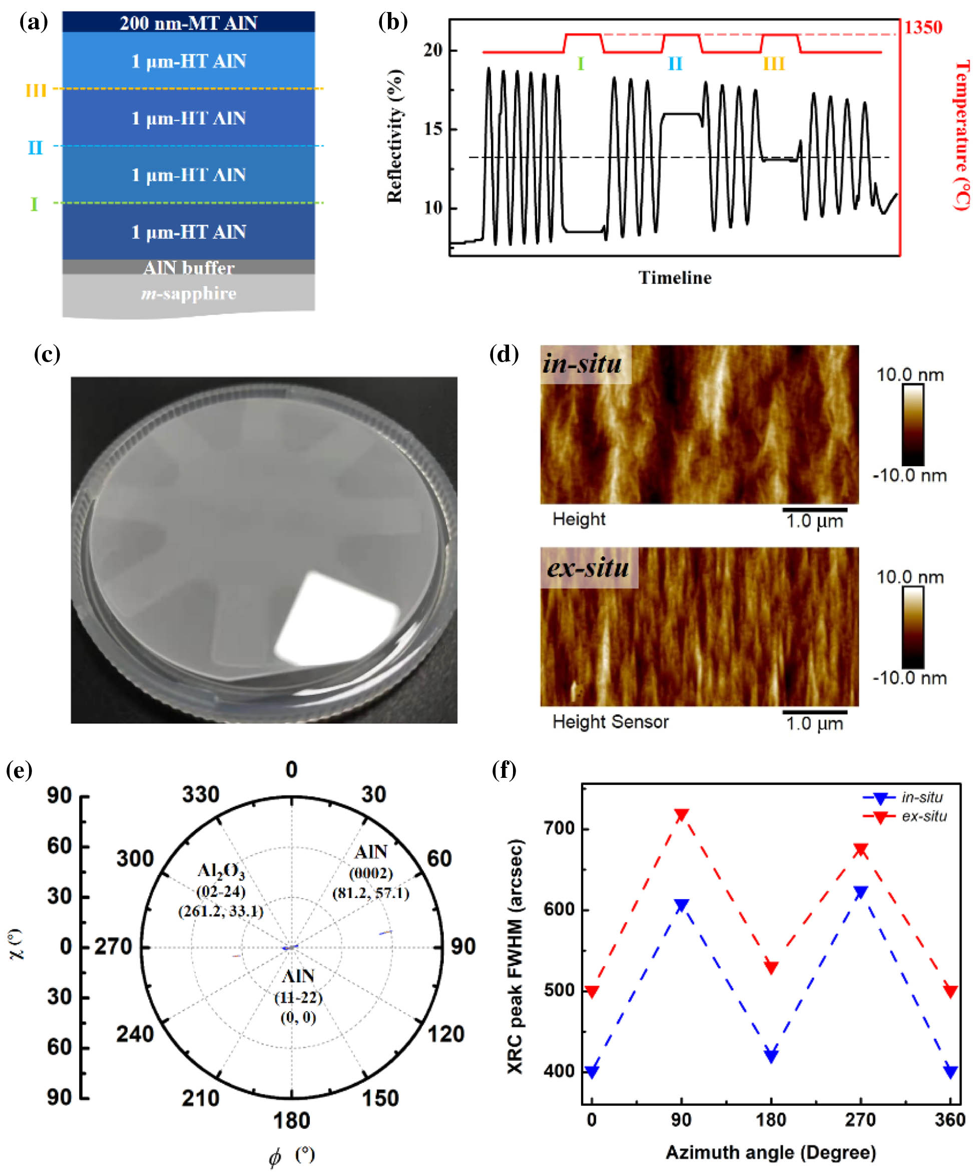
In our newly proposed in situ interface modification method, the semipolar AlN layer is first grown on the -plane sapphire substrate. Pre-deposition nitridation is introduced to form the uniform -oriented AlN epilayer. A low reactor pressure together with a low V/III ratio under an equilibrium growth condition is chosen to achieve a high growth rate of the plane AlN according to the kinetic Wulff plots [10,11]. basal plane stacking faults with a high density are formed during growth due to the lattice mismatch between semipolar AlN and the sapphire substrate. The energetically favorable basal plane stacking faults cannot deform into a glissile partial dislocation, and will penetrate through the crystal without interfaces, grain boundaries, or voids. A high density of stacking faults throughout the epitaxial layers is expected, which will trap the carriers and induce sub-bandgap emission in devices. To avoid the excessive temperature treatment, the intentional introduction of an additional interface to tailor the atomic construction is a good option to block the propagation of stacking faults. The chamber temperature is set to 1350°C, which is slightly higher than the epitaxial temperature to accelerate the surface diffusion and decomposition. According to the calculated phase diagram and absolute surface energy of semipolar AlN, the Al adatom surface construction is most likely to be formed under the Al-rich growing condition [12]. The surface with 8N-6Al adatoms is more favorable for the AlN surface under N-rich ambiance. Therefore, the ambiance was adopted to achieve the N-rich condition [12–15]. The incorporation of N atoms will change the formation enthalpies of post-grown AlN, and thus, the films with fewer stacking faults will benefit from this interface modification. The multi-step in situ interface modification procedure proposes three cycles of modified interfaces, each followed by a 1 μm thick high-temperature AlN layer as shown in Fig. 1(a). The in situ reflectivity spectrum as a function of time and wafer temperature is shown in Fig. 1(b). The AlN epilayer shows a steady surface reflectivity throughout the in situ treated procedure, demonstrating the absence of surface degradation. The mirror-like and crack-free AlN surface with typical semipolar stripe features is obtained in Fig. 1(c).
Figure 1.(a) Schematic structure and (b) wafer temperature and the corresponding surface reflectivity of multi-layer in situ treated AlN. (c) Mirror-like and crack-free in situ treated AlN surface. (d) AFM images of in situ and ex situ treated AlN. (e) Pole figure of AlN , (0002), and sapphire plane diffractions. (f) FWHM of XRC diffraction of AlN templates as a function of azimuth angles.
The surface morphology of in situ treated semipolar AlN is investigated by AFM as shown in Fig. 1(d). For comparison purposes, an AFM image of the AlN thin film subject to conventional ex-situ thermal annealing is also illustrated. The change of surface features and roughness can be attributed to the different annealing processes. Compared with the ex situ annealed AlN, broader stripes with a rough surface are obtained from the in situ treated AlN. The root mean square roughness of the in situ treated AlN is 2.97 nm, larger than that of the ex situ annealed AlN (2.05 nm). The coplanar relationship between the AlN and sapphire substrate is examined by the pole figure as shown in Fig. 1(e). AlN is on-axis, slightly expanding towards AlN (0002) and sapphire directions. AlN (0002) diffraction with lies in the direction of , while sapphire lies in with . The opposite in-plane directions of the (0002) peak of AlN and peak of sapphire reveal that the crystalline relationships of AlN and sapphire are and , respectively. The crystal qualities of AlN subject to both in situ and ex situ treatments were first estimated by the XRCs of diffractions as a function of azimuth angles. The azimuth angle of 0° is defined along the sapphire [0001] direction. As shown in Fig. 1(f), the FWHM values of the XRC peaks of the in situ treated AlN template are lower than those of the ex situ annealed AlN template, suggesting the lower density of stacking faults in the in situ treated AlN layers and consequently less broadening of the diffraction peak. According to the expectation of interface modification by the in situ treated technique, the defects are supposed to be blocked at the modified interface. As a result, the defect density decreases gradually from bottom to top AlN layers. Therefore, it can be concluded that the topmost in situ treated AlN layer has superior crystal quality compared to ex situ annealed AlN, demonstrating that the multi-step in situ interface modification is confirmed as an efficient technique to block the stacking faults. Both in situ and ex situ treated AlN templates exhibit strong anisotropic distribution of dislocations, which is typical in semipolar III-nitrides due to the existence of basal plane stacking faults [16–18]. The in-plane anisotropy can be obtained by calculating the relative proportion of the FWHM values of XRCs with an X-ray beam aligned along direction and direction: where and correspond to the FWHM of XRCs along and directions, respectively. is obtained in the in situ treated AlN, which is slightly larger than the value of the ex situ annealed AlN (). Thus, the smaller anisotropy degree of the ex situ annealed AlN confirms that the stacking faults are annihilated through bulk recrystallization, while interface modification plays a more dominant role in the case of the in situ treatment process, which has less impact on the uniform distribution of defects in the underlying layers.
The extension of stacking faults in the in situ treated AlN layer can be observed through ADF images. Considering the anisotropy distribution of dislocations in the semipolar AlN layer, the samples were sliced along both and planes, and ADF images were collected in and zone axes, respectively. The corresponding diffraction patterns are shown in the inset images of Fig. 2(a). From the ADF images of the AlN layer, a high density of defect lines can be observed in the bottom. These defect lines are basal plane stacking faults of semipolar AlN with an inclined angle of about 55°, most of which disappear beyond the interface of the first in situ treatment process. After the second and third modified interfaces, the density of the defect lines further decreases, leaving behind only several isolated defect lines in the topmost AlN layer. Thus, the proposed in situ interface modification is proved to be an efficient way to block stacking faults. The existence of stacking faults in the bottom layer of in situ treated AlN presents smaller absorption band edges in Fig. 2(b) than the ex situ one due to the slightly narrower bandgaps of stacking faults.
Figure 2.(a) ADF images of in situ treated AlN template taken along and zone axes. (b) Optical transmission spectra and (c) Raman spectra of in situ and ex situ treated AlN templates.
Despite the reduced density of stacking faults, the bulk recrystallization of ex situ annealing can result in a distortion of the AlN lattice with strong compressive strain. The Raman shift is shown in Fig. 2(c). Three main first-order vibration modes [, , and ] can be observed in the range of as the measurement was taken in geometry on the semipolar AlN surface. The A mode and E mode represent the lattice vibrations along the axis and in-plane, respectively. The strain-free position for AlN-like mode is located at [19]. The peak position of the in situ treated AlN shows a slight shift towards a higher wavenumber, suggesting a compressive in-plane strain. The ex situ annealed AlN lattice exhibits a significant shift, which can be attributed to the distorted lattice arrangement via recrystallization. Similarly, the mode also shifts towards a higher wavenumber for two samples. The vibration mode, which represents the strain along the axis, also blueshifts towards a higher wavenumber for the ex situ annealed AlN film, exhibiting a compressed lattice along the axis. The compressed lattice of ex situ annealed AlN film is consistent with the result of the bended and twisted lattice reported in our previous work [4]. Conversely, the in situ interface modification has little influence on the AlN lattice parameter, as the interface modification instead of bulk recrystallization plays a dominant role in defect blocking. Despite the presence of basal plane stacking faults in the bottom AlN layer, the novel multi-step in situ interface modification technique could lead to better crystal quality and much lower residual strain in the AlN template, revealing itself to be a promising candidate for subsequent AlGaN epitaxial growth and device fabrications.
The influence of different AlN templates on the subsequent growth of AlGaN layers and DUV LEDs is further checked. Both in situ and ex situ treated semipolar AlN templates were reloaded into the MOVPE reactor for the growth of the DUV LED structures. The regrown structure contains a thin AlN regrown layer, AlGaN strain relaxation layer with Al composition grading from 0.8 to 0.6 at an interval of 10% Al content, -type , five pairs of MQWs, a 100 nm -type AlGaN layer, and a thin GaN cap layer. Figure 3 shows the symmetric and asymmetric RSM of the DUV LEDs on the different AlN templates. The symmetric RSM was measured with an incident X-ray beam aligned along both and directions. As shown in Figs. 3(a) and 3(b), the peaks are misaligned in symmetric RSM along direction, suggesting the tilt of epitaxial film to compensate for the lattice mismatch; no tilt is found in direction. The tilt angles of AlN are determined from RSM along direction to be 1.79° and 1.10° with respect to the sapphire substrate for in situ and ex situ treated AlN, respectively. A gradually decreased tilt angle can be observed from the bottom to the top of regrown AlGaN layers. The tilt angles of the layers (0.66° and 0.59° for in situ and ex situ treated samples, respectively) are very close to each other. This macroscopic tilt of heteroepitaxy thin film is caused by the formation of misfit dislocation arrays with Burgers vector at the heterointerface [20]. It can be confirmed by ADF images, which will be discussed in detail later. The formation of misfit dislocations is a sign of the relaxation process of large shear stresses of an inclined basal plane. Figure 3(c) shows the asymmetric RSM; the values of the diffraction peaks between two samples are almost identical, suggesting almost the same Al composition of each epilayer. The of the ex situ annealed AlN template is smaller than that of the in situ treated AlN template, consistent with the result of a compressive lattice by Raman spectra. Utilizing the layer tilt angles obtained from the symmetric RSM scan, the peak position of each epilayer in asymmetric RSM scan is corrected and redrawn in Fig. 3(d). The graded AlGaN layers on the in situ treated AlN template present an almost coherent growth mode, whereas the graded AlGaN layers are fully relaxed on the ex situ annealed AlN template. The relaxation of AlGaN is always accompanied by defect formation, demonstrated by the significant broadening of the RSM peak of in the ex situ annealed sample. In contrast, the RSM peak of on in situ treated AlN is relatively narrow, inheriting the high crystal of the AlN template. After the growth of a thick layer, the subsequent MQWs and layers show similar properties of two samples.
Figure 3.() symmetric RSM of semipolar DUV LEDs grown on in situ and ex situ treated AlN templates measured along (a) and (b) directions. (c) () asymmetric RSM of semipolar DUV LEDs on in situ and ex situ treated AlN templates. (d) Adjusted () peak positions of asymmetric RSM according to the different tilt angle of each layer.
To illustrate the defect distribution of post-grown AlGaN layers on in situ and ex situ treated AlN templates, TEM analysis of two samples sliced along both and planes was performed. Figures 4(a)–4(d) show ADF images of two samples along and zone axes. The defect lines in Fig. 4(a) that are inclined at about 55° in the underlying AlN layer can be attributed to basal plane stacking faults. The density of the basal plane stacking faults decreases from the bottom to the top of the in situ treated AlN layer as mentioned above. In the post-grown AlGaN layers, there are still some discontinuous defect lines parallel to the basal plane stacking faults, denoted by in the enlarged image in Fig. 4(a). These inclined defect lines in the zone axis are isolated short lines different from the typical stacking features of basal plane stacking faults. Accordingly, the defect can be attributed to dislocations along the basal plane with Burgers vector components parallel to [0001]. Thus, the multi-step in situ interface modification can efficiently hold back the extension of basal plane stacking faults from the underlying AlN layer. The defect lines denoted by were also found in the AlGaN layer, showing an inclined angle of about 51° with respect to the basal plane, which may originate from the Frank–Shockley partial dislocation with Burgers vector terminating the basal plane stacking faults. The existence of defects and compensates for the strain in AlGaN layers, thus resulting in the gradual relaxation of strains in RSM. At the heterointerface, there is another form of defect denoted by . Defect at the heterointerface is a misfit dislocation causing the tilt of the thin film as mentioned above. This misfit dislocation distributes at the AlGaN interfaces with Burgers vector , which can be hardly found in the ADF image along the zone axis since the contrast of a point at the interface is easily overwhelmed by the atomic Z contrast of different layers. Instead, using ADF images in the zone axis, the misfit dislocation lying in the interface of epilayers can be clearly observed as the lateral defect lines marked by red arrows in Fig. 4(b). The formation of defects contributes to the relaxation of shear stresses between AlGaN layers in the inclined basal plane. In contrast, the ex situ annealed sample exhibits completely different defect line features from the in situ treated sample. As shown in Figs. 4(c) and 4(d), the inclined defect lines along the basal plane in the AlN layer are greatly reduced in the zone axis, but a large number of them still penetrate into the topmost layer, with stacking line features observed in the zone axis. The existence of stacking lines in the AlGaN layer suggests that the basal plane stacking faults are not fully eliminated in the ex situ annealed AlN template. From the view of the zone axis, the recrystallization of AlN under a high temperature of 1700°C results in a high density of chaotic defect lines, showing completely different features from the typical , , and defect features included in Fig. 4(e). There are also lots of extending defects generated from the interface of the regrown AlN and AlGaN layers, contributing to the relaxation of AlGaN layers. The high-density defects in the AlGaN layer on the ex situ annealed AlN template have a strong impact on optical behavior. The PL intensities of the two samples are shown in Fig. 4(f), from which the band edge emission peak of the AlGaN layer can be clearly observed in the in situ treated sample, but not in the ex situ one. Also, the emission from the MQWs of the in situ treated sample is stronger than that of the ex situ. The strong enhancement of luminous intensity with much lower defect density achieved in in situ treated AlGaN LEDs shows a great advantage for the realization of high-efficiency optoelectronic devices.
Figure 4.Overall and enlarged ADF images of DUV LEDs on the in situ treated AlN template along (a) and (b) zone axes. ADF images of DUV LEDs on the ex situ annealed AlN template and the corresponding enlarged images of defects around the interface along (c) and (d) zone axes. (e) Schematic of the transformation of three types of defects, , , and , in AlN and AlGaN layers. (f) PL spectra of DUV LEDs on different AlN templates.
In this work, a multi-step in situ interface modification technique was conducted to achieve high-quality semipolar AlN epitaxial thin film by MOVPE. Inspired by the challenges of strain control and the thermal footprint in the thermal annealing treatment of AlN, the proposed in situ interface modification technique takes advantage of interface modification by enhancing surface diffusion and reconstruction under N-rich ambiance. As a result, basal plane stacking faults in the semipolar AlN epilayer are efficiently blocked. The FWHMs of XRC peaks in the in situ treated AlN templates at all azimuth angles are smaller than in the ex situ face-to-face annealed AlN template. Despite the slightly larger in-plane anisotropy of the distributions of the dislocations, the in situ treated AlN template shows an almost relaxed strain state compared with the highly compressive strains in the ex situ annealed AlN template. The impact of thermal annealing of the AlN template on subsequent AlGaN and DUV LED growth is further studied. The superior performance of the in situ treated AlN acting as a template for DUV LED is readily interpreted by both structural and optical performances of the devices. The post-grown AlGaN layers are coherently grown on top of the in situ treated AlN, inheriting the higher crystal quality of the AlN template and presenting a strong enhancement in luminous intensity. In contrast, many defects are generated from AlGaN on ex situ annealed AlN, degrading the luminescence intensity of device performance. Overall, the multi-step in situ interface modification technique sheds new light on the fabrication of a high-quality semipolar AlN template, providing a promising candidate in the development of high-efficiency optoelectronic devices.
Appendix A
Figure 5.High-resolution TEM images of (a) as-grown and (b) HTA-treated AlN films. (c) Ideal AlN and (d), (e) distorted AlN after high-temperature annealing. (f) Radial distribution function of N atoms around an Al atom by high-temperature annealing.