
Xinxue Wu, Chaolong Fang, Zhihong Li, Yaoju Zhang. Simple and High-Efficiency Preparation Method of Biometric 3D Artificial Compound Eyes for Wide-Field Imaging[J]. Laser & Optoelectronics Progress, 2021, 58(12): 1236001
- Laser & Optoelectronics Progress
- Vol. 58, Issue 12, 1236001 (2021)
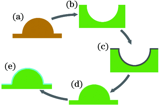
Fig. 1. Preparation flow diagram of flexible sticky macrosphere. (a) Glass convex hemisphere; (b) PDMS concave hemisphere; (c) surface modified PDMS concave hemisphere; (d)(e) PDMS convex hemisphere without mixture film of PDMS prepolymer and its crosslink agent
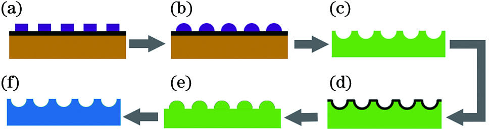
Fig. 2. Preparation process schematic of rigid epoxy resin concave MLA master mold. (a) Photoresist micropillar array; (b) photoresist convex MLA; (c) PDMS concave MLA; (d) surface modified PDMS concave MLA; (e) PDMS convex MLA; (f) rigid epoxy resin concave MLA
Fig. 3. Preparation flow diagram of a 3D ACE. (a) Rigid 2D concave MLA master mold; (b) PDMS film on the rigid 2D concave MLA master mold; (c) squeezing the PDMS dome for adhesion to the PDMS film; (d) schematic of a prepared 3D ACE
Fig. 4. SEM images of 2D and 3D ACEs. (a)(b) SEM images of prepared micropillar and MLA; (c)--(e) SEM image and enlarged SEM images of a 3D ACE formed with a pressure force of 14 N
Fig. 5. Diameter, height, and gap uniformity of ommatidia from center to the edge of the macroeye
Fig. 6. Hemisphere shape under squeezing and removal of squeezing. (a) Side view of a 3D ACE; (b) shape of the hemisphere as it is squeezed with different pressure forces; (c) height and width of the 3D ACE as a function of pressure force
Fig. 7. Imaging properties of the 3D ACE. (a) Clear “A” images from the top of the 3D ACE; (b) clear “A” images from the outer part (in the annulus) of the 3D ACE; (c)(d) larger-magnification “A” images of the lower left and right zones in Fig.7 (b)
Fig. 8. Characterization of the wide FOV of the 3D ACE. (a)--(c) Optical images of focal spots formed by the 3D ACE, inset is an image of a single focal spot; (d) intensity distribution along the x and y axes at an incident angle of 0°; (e) intensity distribution along the x axis at different incident angles; (f) intensity distribution along the y axis at different incident angles
|
Table 1. Parameters of a micropillar array (MPA), 2D ACE, and 3D ACE

Set citation alerts for the article
Please enter your email address
© Copyright 2018-2021 | Chinese Laser Press. All Rights Reserved 沪ICP备15018463号-20