
Dongshi Zhang, Koji Sugioka. Hierarchical microstructures with high spatial frequency laser induced periodic surface structures possessing different orientations created by femtosecond laser ablation of silicon in liquids[J]. Opto-Electronic Advances, 2019, 2(3): 190002
- Opto-Electronic Advances
- Vol. 2, Issue 3, 190002 (2019)
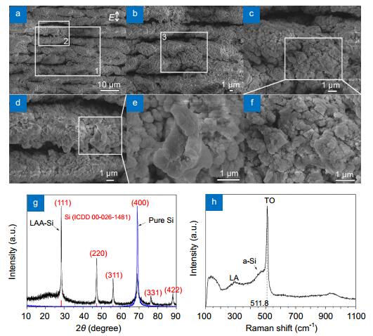
Fig. 1. SEM images of surface structures under different magnifications (a–f), and XRD (g) and Raman (h) spectra of the Si prepared by LAA with a laser fluence of 3.8 J/cm2, a line interval of 5 μm and a scanning speed of 1 mm/s.(a ) Overview morphology of the grooves generated by LAA. (b ) Enlarged SEM image of the grooves in region 1 in (a ). (c ) Enlarged SEM images of region 3 in (b ), which is composed of microislands. (d ) Enlarged SEM image of region 2 in (a ), showing a microstructure on the crest of a groove. (e , f ) Enlarged SEM images of the regions enclosed in squares in (d ) and (c ), respectively. The direction of light polarization is indicated in (a ).
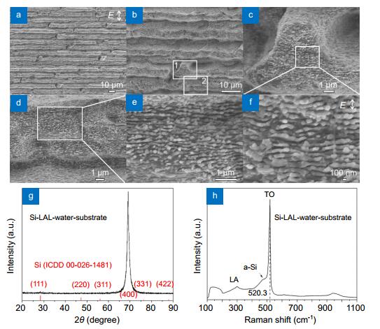
Fig. 2. SEM images (a–f), XRD (g) and Raman (h) spectra of Si surfaces prepared by laser ablation in water with a laser fluence of 1.7 J/cm2, a line interval of 5 μm and a scanning speed of 1 mm/s.(a ) Overview morphology of the grooves generated by LAL in water. (b ) Enlarged SEM image of parallel and bifurcated grooves. (c ) Enlarged SEM image of the bifurcated crest of a groove in region 1 in (b ), and (d ) enlarged SEM image of the valley of a groove in region 2 in (b ), which shows Si HSLFs on top. (e , f ) Enlarged SEM images of the regions enclosed in open squares in (d ) and (c ), respectively. The direction of light polarization is indicated in (a ) and (f ).
Fig. 3. SEM images (a–f), XRD (g) and Raman (h) spectra of Si surfaces prepared by laser ablation of Si in acetone with a laser fluence of 1.7 J/cm2, a line interval of 5 μm and a scanning speed of 1 mm/s.(a ) Overview morphology of the grooves generated by LAL in acetone. (b ) Enlarged SEM images of the random microscale protrusions. (c ) Enlarged SEM image of one of the microprotrusion located in region 1 in (b ). (d ) Enlarged SEM image of the crest of a microscale protrusion located in region 2 of (b ), where Si-HSFLs were formed. (e ) Enlarged SEM image of the valley of a microstructure located in region 3 in (b ), where Si-HSFLs were also formed. (f ) Enlarged SEM image of Si-HSFL structures on the side wall of the microstructures in (c ). Light polarization direction is indicated in (a ) and (f ).
Fig. 4. Comparison of the Raman spectra of Si surfaces prepared by laser ablation in air, water and acetone.
Fig. 5. (a–c) Schematics of the proposed ablation scenarios in air, water and acetone, respectively.
Fig. 6. TEM images of (a–c) large and (d–f) small particle networks synthesized by LAA. (g) Size distribution of small particles.
Fig. 7. TEM images of (a–c) large particles and networks and (d–f) small particles synthesized by LAL in water. (g) Size distribution of small particles
Fig. 8. TEM images of (a–c) large and (d–f) small particle networks synthesized by LAL in acetone. (g) Size distribution of small particles.
Fig. 9. SEM images of structures obtained by LAL of Si in water at scanning speed of (a–c) 0.1, (d–f) 0.5, (g–i) 1 and (j–l) 2 mm/s with a scanning line interval of 15 μm.Parallel grooves obtained by LAL at 0.1 and 0.5 mm/s where some grooves were destroyed, presumably due to shockwaves. (b , e , h , k ) Enlarged SEM images of grooves, and (c , f , i , l ) closeup observation of Si-HSFLs. The polarization direction of light is indicated in (c , f , I , l ). The scanning direction is perpendicular to the direction of light polarization.
Fig. 10. SEM images of the structures obtained by LAL of Si in water at scanning speed of (a–c) 0.1, (d–f) 0.5, (g–i) 1 and (j–l) 2 mm/s with a scanning line interval of 20 μm.(a ) Parallel grooves obtained by LAL at 0.1 mm/s where some grooves were destroyed probably owing to shockwaves. (d , g , j ) Grooves obtained by LAL at 0.5, 1 and 2 mm/s, are no longer parallel owing to liquid fluctuation caused by high speed scanning. (c , f , i , l ) The polarization direction of light is indicated in (b , c , f , i , l ). The scanning direction is perpendicular to the direction of light polarization.
Fig. 11. Raman spectra of Si substrates ablated with line intervals of 15 μm (a) and 20 μm (b) at scanning speeds of 0.1, 0.5, 1 and 2 mm/s.The a-Si peak was marked in each Fig. to demonstrate the ubiquitous melting phenomena observed during LAL.
Fig. 12. SEM images of micro-structures obtained by LAL of Si in water with a line interval of 15 μm (a–f) at scanning speeds of 0.1 mm/s (a–c), 0.5 mm/s (d–f), 2 mm/s (g–i) and a line interval of 20 μm at a scanning speed of 0.1 mm/s (j–o).(b , e , h ) Enlarged SEM images of the broken groove, the side wall of groove and the fluctuated microstructures in (a, d, g), respectively, where tilted Si-HFSLs are observed, as more clearly shown in further enlarged SEM image in (c, f, i). (k , n ) Enlarged SEM images of a groove side wall and the crest of a broken groove in (j, m), respectively, where clockwise- and anti-clockwise-tilted Si-HFSLs are observed, as seen more clearly in further enlarged SEM images in (l, o). (o ) Enlarged SEM image of region enclosed by open square in (n) shows that Si-HSFLs also form in the deep cavity. The tilt angles of Si-HSFLs with respect to the expected horizontal direction (i.e., perpendicular to direction of light polarization) of LIPSSs are indicated.
Fig. 13. SEM images of the hierarchical micro/nanostructures obtained by LAL of Si in water with a line interval of 20 μm at scanning speeds of 0.1 (a–c), 0.5 (d–f), 1 mm/s (g–i) and 2 mm/s (j–o).(b , e , k ) Enlarged SEM images of the crests of grooves in (a, d, j), respectively, where Si-HFSLs whose orientation directions are perpendicular to those of the grooves are observed. (c , f , l ) Further enlarged SEM images of the regions enclosed in open squares in (b, e, k), respectively. (h , n ) Enlarged SEM images of the valleys of the grooves in (g, m), respectively, where Si-HFSLs are also observed, as more clearly shown in the further enlarged SEM images in (i, o). (k , m ) Enlarged SEM images of the crest and the valley of the grooves of regions 1 and 2 in (j), respectively. Irregular grooves generated at 0.5 mm/s are marked by arrows in (d). Owing to the more chaotic bubble dynamics during LAL at 0.1 and 1 mm/s, the grooves generated in (a) and (g) are irregular. The scanning direction is parallel to the direction of light polarization. The light polarization direction is marked in (c, f, i, l, and o).
Fig. 14. SEM images of micro/nano structures obtained by LAL of Si in water with a line interval of 20 μm at scanning speeds of 0.1 (a–f) and 1 mm/s (g–l).(b , c ) Enlarged SEM images of the Si-HSFLs of regions 1 and 2, respectively, on the adjacent mountain-like structures in (a), respectively. (e , f ) Enlarged SEM images of the Si-HSFLs of regions 1 and 2, respectively, on the side walls of the mountain-like microstructures in (d). (h , g ) Enlarged SEM images of the Si-HSFLs of regions 1 and 2, respectively, at the bottom of the mountain-like microstructures in (d). (b , e , h ) The tilted angles of Si-HSFLs as compared to the expected horizontal direction (perpendicular to light polarization) of Si-HSFLs (c, f, and i) are marked. (k , l ) Enlarged SEM images of the nanostructures of regions 1 and 2 in (j), respectively, which indicate the splash of molten layers and simultaneous modulation into nanoripples. Light polarization direction is marked in (a, c, f, I, and l).
| ||||||||||||||||||||||||||||||||||||||||||||||||||||||||||||||||||||||||||||||||||||||||||||||||||||||||||||||||||||||||
Table 1. Summary of fs-LIPSSs formed on silicon substrates by laser ablation in water, acetone, oil, air and vacuum using different parameters, in the present and previous studies.


Set citation alerts for the article
Please enter your email address

© Copyright 2018-2021 | Chinese Laser Press. All Rights Reserved 沪ICP备15018463号-20