Abstract
High spatial frequency laser induced periodic surface structures (HSFLs) on silicon substrates are often developed on flat surfaces at low fluences near ablation threshold of 0.1 J/cm2, seldom on microstructures or microgrooves at relatively higher fluences above 1 J/cm2. This work aims to enrich the variety of HSFLs-containing hierarchical microstructures, by femtosecond laser (pulse duration: 457 fs, wavelength: 1045 nm, and repetition rate: 100 kHz) in liquids (water and acetone) at laser fluence of 1.7 J/cm2. The period of Si-HSFLs in the range of 110–200 nm is independent of the scanning speeds (0.1, 0.5, 1 and 2 mm/s), line intervals (5, 15 and 20 μm) of scanning lines and scanning directions (perpendicular or parallel to light polarization direction). It is interestingly found that besides normal HSFLs whose orientations are perpendicular to the direction of light polarization, both clockwise or anticlockwise randomly tilted HSFLs with a maximal deviation angle of 50° as compared to those of normal HSFLSs are found on the microstructures with height gradients. Raman spectra and SEM characterization jointly clarify that surface melting and nanocapillary waves play important roles in the formation of Si-HSFLs. The fact that no HSFLs are produced by laser ablation in air indicates that moderate melting facilitated with ultrafast liquid cooling is beneficial for the formation of HSFLs by LALs. On the basis of our findings and previous reports, a synergistic formation mechanism for HSFLs at high fluence was proposed and discussed, including thermal melting with the concomitance of ultrafast cooling in liquids, transformation of the molten layers into ripples and nanotips by surface plasmon polaritons (SPP) and second-harmonic generation (SHG), and modulation of Si-HSFLs direction by both nanocapillary waves and the localized electric field coming from the excited large Si particles. Introduction
Laser ablation offers a versatile platform that can simultaneously induce surface structures1-3 and synthesize nanomaterials4-13 for diverse applications, such as wettability control14-17, bioimaging6, 18, cellular growth manipulation19-21, lithium-ion batteries22, surface enhanced Raman scattering (SERS) detection23, 24, catalysis/ photocatalysis/electrochemical-catalysis6, 7, 25 and anti- friction26-29. Laser processing also enables the microfabrication of three-dimensional structures and devices30, 31. In the large variety of subfields related to laser ablation and laser processing, laser induced periodic surface structures (LIPSS) which can be formed on almost any kinds of materials (e.g. metal, glass, polymer and semiconductor) with tunable periods and functions has been an evergreen topic since its discovery by Birnbaum in 196532. According to the relative period (ΛLIPSS) of LIPSS as compared to the laser wavelength (λ0), LIPSS is classified into low spatial frequency LIPSS (LSFLs) with a periodicity close to or slightly smaller than the laser wavelength and high-spatial frequency LIPSS (HSFLs) with a periodicity much smaller than the laser wavelength1.
HSFLs is easily achievable by femtosecond (fs) laser ablation. However, environments such as air, vacuum and liquids, greatly influence the periods of the LIPSS. Taking silicon as an example, except for a few reports that demonstrated the feasibility of obtaining silicon HSFL (Si-HSFL) with a very small pulse energy of ~3 nJ/pulse at a high laser repetition rate of 80 or 90 MHz33, 39, 42, only LSFLs were obtained through fs laser ablation in air (fs-LAA)34, 35 or vacuum36, 37, as shown in Table 1. In contrast, Si-HSFL is much more easily obtained by fs laser ablation in liquids (fs-LALs), as clearly seen in Table 1. For example, at laser fluences just above the ablation thresholds, the periodicities of Si-LIPSS obtained in water and air were 120 nm and 670 nm, respectively38. Harzic et al. showed that the period of Si-LSFL produced by fs-LAA was 800-900 nm, close to the wavelength (1040 nm), but the period of LIPSS obtained by fs laser ablation of Si in oil was 70-100 nm, much smaller than the 800-nm laser wavelength39. Similarly, Derrien et al. found that Si-HSFLs with a ΛLIPSS of 0.15 × λ0 were obtainable by laser ablation in water, while only Si-LSFL with a ΛLIPSS of 0.70×λ0 was obtained in air40. Daminelli et al. showed that laser ablation in water at laser fluence of 1.5 J/cm2 (1000 pulses, wavelength of 800 nm and pulses duration of 130 fs) generated Si-HSFL with a period of 100 nm, while LAA under the same conditions except for a laser fluence of 0.45 J/cm2 only yielded LSFLs41. A number of mechanisms have been proposed to explain the reduction in the period of LIPSS via LAL, including the excitation of surface plasmon polaritons (SPP)40 and second-harmonic generation (SHG)42. However, although some insights have been given, the detailed mechanisms remain unclear; more experimental evidence is needed for better clarification.
| Environment | Scan method | Ripple periodicity (nm) | Laser parameters (pulse duration, wavelength, repetition rate, fluence) and liquid thickness | Ref. |
| Line-by-line means line ablation with multiple scanning with a line overlap of Δd of the space between adjacent lines. |
| Water, acetone | Line-by-line | 110–200 | 457 fs, 1045 nm, 100 kHz, 1.7 J/cm2, 5 mm thickness | This work |
| Acetone | Line-by-line | 120–220 | ~40 fs, 800 nm, 1 kHz, 0.35–0.62 J/cm2, ~7 mm thickness | 50 |
| Water | Line-by-line | 120 | 100 fs, 800 nm, 1 kHz, 0.3–0.5 J/cm2, 10 mm thickness | 43 |
| Water | Crater ablation | 120 | 100 fs, 800 nm, 1 kHz, 0.163 J/cm2, 10 mm thickness | 38 |
| Water | Line-by-line | 140–150 | 150 fs, 800 nm, 10 Hz, 0.55–0.88 J/cm2, 4 mm thickness | 20 |
| Water | Crater ablation | 150–400 | 100 fs, 800 nm, 1 kHz, 0.12–0.14 J/cm2, 2 mm thickness | 46, 47 |
| Water | Line-by-line | 90 | 35 fs, 800 nm, 1 kHz, 0.14 J/cm2, 5 mm thickness | 51 |
| Water | Crater ablation | 80–130 | 30 fs, 790 nm, 1 Hz, 0.09 J/cm2, 5 mm thickness | 40 |
| Water | Crater ablation | ~ 100 | 130 fs, 800 nm, 10 Hz, 1.5 J/cm2, 5 mm thickness | 41 |
| Oil | Line | 70–100 | 350 fs, 800 nm, 90 MHz, 3.5 nJ/pulse | 39 |
| Air | Crater ablation | 520–620 | 30 fs, 790 nm, 1 Hz, 0.17 J/cm2 | 40 |
| Air | Crater ablation | 670 | 100 fs, 800 nm, 1 kHz, 0.2 J/cm2 | 38 |
| Air | Line | 500 ± 40 | 3.5 fs, 760 nm, 1 kHz, 0.3 J/cm2 | 52 |
| Air | Line | 800–900 | 350 fs, 1040 nm, 10 kHz, 1 μJ/pulse | 39 |
| Air | Line | 110–160 | 140 fs, 80 MHz, 690–950 nm, 3.1 nJ/pulse | 33 |
| Air | Line-by-line | 600–700 | 50 fs, 800 nm, 1 kHz, 0.21 J/cm2, 800 μm/s, Δd=10 μm | 53 |
| Air | Line-by-line | 120±10 | 170 fs, 80 MHz, 700–950 nm, 3 nJ/pulse, 1 mm/s, Δd=1 μm | 42 |
| Air | Crater ablation | 750, 1130 | 150 fs, 775 nm, 1 kHz, 0° and 45° beam tilt, 80 nJ/pulse | 35 |
| Air | Single line | 800–900; 70–100 | 350 fs, 1040 nm, 10 kHz, 1 μJ/pulse; 170 fs, 800 nm, 90 MHz, 3.5 nJ/pulse | 39 |
| Air | Crater ablation | 700–1200 | 125 fs, 800 nm, 1 kHz, 0.8 J/cm2 | 34 |
| Vacuum | Crater ablation | ≈ 200 and 600–700 | 100 fs, 800 nm, 1 kHz, 60 000 pulses at 0.4×10¹² W/cm2 pulses 20000 pulses at 1.6×10¹² W/cm2 | 36 |
| Vacuum | Crater ablation | 720–750 | 430 fs, 800 nm, 1 kHz, 0.37 J/cm2 | 37 |
Table 1. Summary of fs-LIPSSs formed on silicon substrates by laser ablation in water, acetone, oil, air and vacuum using different parameters, in the present and previous studies.
Whether in air, vacuum or liquid, Si-HSFLs with small periodicities can be produced in a "gentle" ablation regime at low laser energy/power/fluence. As shown in Table 1, Si-HSFLs with a small periodicity (Λ=70-200 nm, about a quarter of the laser wavelength or even smaller) were observed at low fluence (0.4-1 J/cm220, 43, 0.2 J/cm244), near the ablation threshold of Si (0.28±0.3 J/cm245), at lower pulse energy (3.5 nJ/pulse39) or lower power density (0.4×10¹² W/cm236), irrespectively of the scan method (line-by-line or static crater ablation). Increasing the laser fluence/power increases the period of the ripples39. Once "strong" laser ablation is initiated at high laser fluences, Si-HSFLs completely disappear and are replaced by microcale structures46 because of strong thermal effects, which completely inhibits fine structure formation47. Shen et al. showed that Si-HSFL was achievable at low laser fluences in the 0.3-0.5 J/cm2 range but not at 3.5 J/cm2, even in water43. Miyaji et al. also found Si-HSFLs with ΛLIPSS of ~150 nm was only achievable by laser ablation in water with fluences in the range of 0.12-0.14 J/cm2 and increasing laser fluence to 0.15 J/cm2 completely enlarged the ΛLIPSS of Si-HSFLs to 400 nm46. Differently, Daminelli et al. demonstrated the possibility to generate Si-HSFL with ΛLIPSS of ~100 nm at the edge of a crater created by LAL in water at fluence of 1.5 J/cm241. Yiannakou et al. showed that Si-HSFL can still form at fluence of 0.55±0.10 J/cm2 and increasing laser fluence to 0.62±0.14 J/cm2 gave rise to the formation of micro-grooves, leading to the formation of micro/nano dual scale hierarchical structures20. The summary of previous works shown in Table 1 indicates Si-HSFLs are achievable in the wide laser fluence range of 0.1-1.5 J/cm2. Generally, ablation of Si at higher fluences produces microgrooves48 or microstructures49. Hence, it is wondered whether HSFLs can be imparted on the microgrooves or different microstructures. If so, whether the orientations of Si-HSFLs are still perpendicular to the direction of light polarization, as those of Si-HSFLs obtained by LAL at low fluences40, 46, 47, is still questionable.
In light of few reports on hierarchical microstructures with nanoscale Si-HSFLs, the present work intends to explore and increase the varieties of hierarchical microstructures with Si-HSFL by LAL at laser fluences well above the ablation threshold. For a better demonstration of the effects of environments on Si-HSFL formation, LAL (in both water and acetone) and LAA are, respectively, performed while keeping the pulse energy constant at 6 μJ/pulse. The fluences used for LAL and LAA are estimated to be 1.7 and 3.8 J/cm2, respectively. To explore whether Si-HSFL depends on the number of pulses acting on the same ablation area, scanning speeds of 0.1, 0.5, 1 and 2 mm/s (the corresponding specific pulse numbers for a single scan line with a distance of 1 mm are 1×10⁶, 2×10⁵, 1×10⁵, 5×10⁴, respectively) and scanning line intervals of 5, 15 and 20 μm are adopted. To tailor the relative directions of Si-HSFLs as compared to that of their underlying microgrooves, scanning directions parallel and perpendicular to the light polarization direction are both used. The morphologies of the surface structures are characterized by scanning electron microscopy (SEM), and the compositions of the ablated substrates are characterized by Raman and X-ray diffraction (XRD) spectrometry. The nanomaterials synthesized as by-products which shed light on what occurs during LAL and LAA are examined by TEM. First, LAA and LAL are carried out at the line interval of 5 μm at a scanning speed of 1 mm/s for an analysis of the synthesized nanomaterials to elucidate ablation dynamics and meanwhile demonstrating the effect of environment on HSFL formation. Then, Si-HSFLs obtained by LAL in water at different scanning speeds and line intervals are analyzed. Finally, on the basis of a comparison of our results with the literature, a synergistic mechanism is proposed for Si-HSFL formation by LAL at high fluences and the critical factors are discussed.
Experimental
An fs laser system (FCPA μ Jewel D-1000-UG3, IMRA America Inc., Ann Arbor, MI, USA) with a pulse duration, wavelength and repetition rate of, respectively, 457 fs, 1045 nm and 100 kHz was used for laser ablation. The laser beam was focused by a 20 × objective lens (numerical aperture: 0.4, Mitutoyo, Kawasaki, Japan). Single-crystalline silicon (c-Si) substrates (20×20×1 mm) with a p(100) orientation were placed inside a glass chamber. For LAL, the glass chamber was filled with 10 mL of water or acetone with a liquid thickness of 5 mm above the target surface. An area of 3.5 mm× 3.5 mm was scanned using the line-by-line method described in refs.14-16 with a line interval of 5 μm and a scanning speed of 1 mm/s. The scanning direction was perpendicular to the light polarization direction. The laser power was set at 600 mW which is equivalent to pulse energy (E) of 6 μJ/pulse at a 100 kHz repetition rate. The spot sizes (2w0) for laser ablation in air, water and acetone were experimentally measured as 20, 30 and 30 μm. According to the equation of fluence F=2E/πw02 which generated laser fluences of 3.8, 1.7 and 1.7 J/cm2, respectively. To prevent random ablation, the sticky bubbles generated during LAL in water were removed in time using a syringe. The bubbles in acetone did not adhere to the substrates, disappearing readily before the arrival of the succeeding laser pulse. To examine the effect of the number of pulses on Si-HSFLs, LAL of Si was performed in water with line intervals of 15 and 20 μm at scanning speeds of 0.1, 0.5, 1 and 2 mm/s, in which cases the specific pulse numbers for a single scan line with a distance of 1 mm are 1×10⁶, 2×10⁵, 1×10⁵, 5×10⁴, respectively. For LAL using water, scanning was also performed parallel to the light polarization direction at scanning speeds of 0.1, 0.5, 1, to 2 mm/s and a line interval of 20 μm. During scanning at 0.5 and 2 mm/s, the sticky bubbles on the grooves could be removed by a syringe, while at 0.1 and 1 mm/s, the sticky bubbles were not removed in time due to the loose of the tip of the syringe so that the pressure exerted to the sticky bubble were not strong enough to remove them, which yielded very different microstructures in these two scanning speed regimes. After LAA, the nanomaterials were transferred directly into a glass bottle by gently scraping the deposits using a polymer plate. Then, the ablated target was cleaned successively in water and acetone for 5 min each. In all LALs runs, some droplets of colloids were used for TEM sample preparation, while other colloids were stored directly in glass bottles. The compositions of the ablated substrates and the synthesized nanomaterials were analyzed by XRD (Rigaku, CuKα radiation [40 kV-30 mA], SmartLab-R3kW, Tokyo, Japan) and Raman spectroscopy (LabRAM, Hiriba, He-Ne laser, 632 nm, 0.686 mW, Tokyo, Japan). Two SEMs (Jeol6330, Tokyo, Japan, and Thermo Fisher Scientific, Quattro ESEM, Tokyo, Japan) were used to characterize the micro- and nanostructures of the ablated substrates. A TEM microscopy (Jeol, JEM-1230, Tokyo, Japan) operating at 80 kV was used to analyze the morphologies of the synthesized nanomaterials.
Results and discussion
Structural difference in air, water and acetone
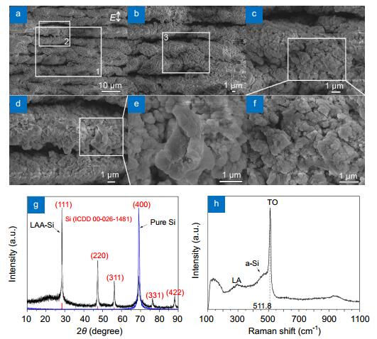
Figures 1-3 show the morphologies, the XRD and Raman spectra of Si surfaces laser-ablated in, respectively, air, water and acetone at laser fluences of 3.8 J/cm2 for LAA and 1.7 J/cm2 for LAL with a line interval of 5 μm and a scanning speed of 1 mm/s. A comparison of these results reveals many differences, in particular, significant environment-dependent morphological differences. Hierarchical structures composed of periodic microgrooves decorated with patched structures were produced by LAA (Figs. 1(a)-1(f)). These microgrooves resulted from line-by-line scanning of the focused laser beam (Figs. 1(a) and 1(b)). Some microgrooves were filled with microislands presumably owing to thermal effects (Figs. 1(c) and 1(f)), while irregular structures with smooth patched surfaces were formed on the bumps (Figs. 1(d) and 1(e)). No LIPSSs were formed by LAA.

Figure 1.SEM images of surface structures under different magnifications (a–f), and XRD (g) and Raman (h) spectra of the Si prepared by LAA with a laser fluence of 3.8 J/cm2, a line interval of 5 μm and a scanning speed of 1 mm/s.(a) Overview morphology of the grooves generated by LAA. (b) Enlarged SEM image of the grooves in region 1 in (a). (c) Enlarged SEM images of region 3 in (b), which is composed of microislands. (d) Enlarged SEM image of region 2 in (a), showing a microstructure on the crest of a groove. (e, f) Enlarged SEM images of the regions enclosed in squares in (d) and (c), respectively. The direction of light polarization is indicated in (a).
Figure 2.SEM images (a–f), XRD (g) and Raman (h) spectra of Si surfaces prepared by laser ablation in water with a laser fluence of 1.7 J/cm2, a line interval of 5 μm and a scanning speed of 1 mm/s.(a) Overview morphology of the grooves generated by LAL in water. (b) Enlarged SEM image of parallel and bifurcated grooves. (c) Enlarged SEM image of the bifurcated crest of a groove in region 1 in (b), and (d) enlarged SEM image of the valley of a groove in region 2 in (b), which shows Si HSLFs on top. (e, f) Enlarged SEM images of the regions enclosed in open squares in (d) and (c), respectively. The direction of light polarization is indicated in (a) and (f).
Figure 3.SEM images (a–f), XRD (g) and Raman (h) spectra of Si surfaces prepared by laser ablation of Si in acetone with a laser fluence of 1.7 J/cm2, a line interval of 5 μm and a scanning speed of 1 mm/s.(a) Overview morphology of the grooves generated by LAL in acetone. (b) Enlarged SEM images of the random microscale protrusions. (c) Enlarged SEM image of one of the microprotrusion located in region 1 in (b). (d) Enlarged SEM image of the crest of a microscale protrusion located in region 2 of (b), where Si-HSFLs were formed. (e) Enlarged SEM image of the valley of a microstructure located in region 3 in (b), where Si-HSFLs were also formed. (f) Enlarged SEM image of Si-HSFL structures on the side wall of the microstructures in (c). Light polarization direction is indicated in (a) and (f).
In contrast, clearer microgrooves (Fig. 2(a)), though bifurcated at some points (Figs. 2(b) and 2(c)), were produced in water. Both the crests (Figs. 2(c) and 2(f)) and valleys (Figs. 2(d) and 2(e)) of the groove structures were covered by HSFLs having periods of 120-200 nm and lengths of 700-6000 nm, and oriented perpendicular to the laser polarization direction. In acetone, hierarchical structures composed of random microscale protrusions (Figs. 3(a)-3(c)) textured with HSFLs with periods of 110-200 nm were generated. These were discovered on all crests, valleys, and side walls of the microprotrusions (Figs. 3(d)-3(f)). The HSFL periods and directions were almost the same as those obtained in water. However, the lengths of the HSFLs were much shorter, ranging from ~500 nm to 2 μm owing to the limited lengths of the microprotrusions along the HSFL direction. The asymmetry and bifurcation of the micro-structures is attributable to the chaotic bubbles generated by LAL in a batch chamber6, 54, which causes random beam reflection and refraction. Even with the help of a liquid flow to reduce the density of sticky bubbles on the surfaces, chaotic ablation cannot be prevented completely55. Previous studies have shown that successive fs laser ablation of Si in water at low laser fluence43 and the successive irradiation at moderate fluences20 (0.6-0.9 J/cm2) can generate hierarchical micro beads decorated with HSFLs with a periodicity of 120-150 nm. The present work demonstrates that single-step LAL of Si at high fluence offers an alternative approach to developing large-scale hierarchical structures with both crests and valleys decorated by HSFLs.
Comparing the XRD spectra of the Si surfaces treated by LAA and LAL reveals how the ablation environment affects the crystallinity. In the case of LAA, poly Si (p-Si) dominated the phase of the substrates (Fig. 1(g)), which indicated that laser ablation significantly poly-crystallized the c-Si substrate (blue curve in Fig. 1). The broad band centered at 2θ=23° in the XRD spectrum (Fig. 1(g)) indicates the formation of amorphous Si (a-Si). In the case of LAL (both water and acetone), the intrinsic (400) peak was broadened and a very low-intensity peak indexed to the (111) crystal plane of p-Si (ICDD 00-026-1481) appeared (Fig. 2(g) and Fig. 3(g)), which indicated that LAL-induced poly-crystallization was much lower than that induced by LAA. Also, no band of the a-Si phase was observed from the LAL substrates, which indicated that LAL significantly inhibited the thermal effect. This result is consistent with previous findings55. However, for all three substrates, the featured Raman frequency (ω) bands at 480 cm-1 associated with a-Si were detected in Raman spectra (Figs. 1(h), 2(h) and 3(h)), which was indicative of the ubiquitous occurrence of melting behavior during laser ablation regardless of the ablation environment. For a more detailed comparison, the enlarged Raman spectra bands (400-600 cm-1) of the ablated substrates in different environments are shown together in Fig. 4. The Raman peak intensity of a-Si for LAL is much smaller than that for LAA. This suggests that the melting zone/depth induced by LAL is much shallower than that of LAA. That is why no peak of a-Si was detected for LAL during XRD characterization. The Raman band at 520 cm-1 corresponds to the transverse-optic (TO) phonon mode of Si crystallites. If the crystallites' sizes decrease, the TO band would blueshift to a lower wavenumber56. In acetone, although the TO mode is located at 520.3 cm-1, the TO peak becomes asymmetric and broader with a full width at half maximum (FWHM) of 4.8 cm-1, which can be attributed to the formation of p-Si. Even though the substrate obtained by LAL in water has the same TO position as that obtained in acetone (520.3 cm-1), the TO mode of LAL- water substrate becomes more asymmetric and its width is much broader with a FWHM of 12 cm-1, in accordance with previous reports57. This indicates that the p-Si generated in water has a much broader size distribution than that generated in acetone. In the case of LAA, the TO mode blue-shifts to 511.8 cm-1 with a FWHM of 12 cm-1, which could be due to the particles decorating the formed micro-grooves. The particle size is theoretically predicted to be around 3.6 nm on the basis of the Raman peak at 511.8 cm-158. The Raman analysis and XRD results clearly suggest that, within the detection depths of both Raman spectroscopy and XRD characterizations, the majority of Si substrates were altered by LAA, but only a little altered by LAL, which indicates that the heat- affected zone (HAZ) induced by laser ablation decreases according to the environment, in the order air > water > acetone (Fig. 5), similarly to the particle productivity obtained by laser ablation in different environments6, 55, 59. In air, because of strong thermal effects, molten particles are ejected from the substrate and result in the deposition of particles near the ablated areas (Fig. 5(a)). During LAA, the dense plasma induces the formation of high-pressure shockwaves inside the ablated substrates, which combined with the strong thermal effect, triggering the poly-crystallization of c-Si into p-Si. In the case of LAL in water (Fig. 5(b)), benefiting from the superfast cooling of molten layers in liquid atmosphere, the HAZ for LAL in water (Fig. 5(b)) would be expected to be much smaller than that for LAA. In addition, because of the consumption of laser energy by water breakdown and the attenuation of the energy of incident pulses during their propagation in liquids6, the effective pulse energy used in LAL is actually lower than that used in LAA so that the poly-crystallization rate is much lower in the case of LAA. The ejected large molten droplets resulting from thermal effects and the small particles produced by phase explosion60 disperse well in water. In the case of LAL in acetone (Fig. 5(c)), since acetone decomposition10, 11, 13, 61 consumes more laser energy, the effective laser energy for ablation is reduced. As a result, the poly-crystallization rate is further reduced (see Fig. 4), in accordance with the literature, which has shown that the kerf width gradually decreases with increasing ethanol ratio of ethanol-water mixtures used for LAL55. The difference in the XRD and Raman spectra of LAL and LAA substrates indicates that p-Si formation is not the main factor governing HSFL formation; rather, the evidence suggests that the moderate melting during LAL as compared to the strong melting during LAA must be related to HSFL formation. This conclusion is consistent with a report by Sedao et al. who have proposed that surface melting and resolidification play important roles in HSFL formation on the basis of Ni(111) targets irradiated at low fluence62.
Figure 4.Comparison of the Raman spectra of Si surfaces prepared by laser ablation in air, water and acetone.
Figure 5.(a–c) Schematics of the proposed ablation scenarios in air, water and acetone, respectively.
Examination of ablation dynamics
To determine the ablation dynamics, specifically, whether melting occurs in the ablated substrates for all cases, the TEM morphologies of the nanomaterials synthesized by laser ablation in different environments were characterized, as shown in Figs. 6-8. Even though the particle morphologies were different, all nanomaterials could be classified into two categories: large particle networks and small particles, with a very large size difference. The nanomaterials synthesized in air exhibited unusual structures, such as microparticle islands with a check-mark structure (Fig. 6(a)), submicro-particles with long tails (Fig. 6(b)), and a tree-like structure (Fig. 6(c)). The formation of particle islands and trees during LAA is attributable to (1) the spontaneous fusion of different particles when they encounter each other in molten states and (2) the annealing effect within the HAZ induced by subsequent laser irradiation after they are deposited on the substrate. In addition to large structures, web-like structures with lengths of hundreds of nm and width of 5-7 nm were also produced (Figs. 6(d)-6(f)). The web-like structures contained particles with average sizes of 25.2±14.3 nm (Fig. 6(g)).
Figure 6.TEM images of (a–c) large and (d–f) small particle networks synthesized by LAA. (g) Size distribution of small particles.
Figure 7.TEM images of (a–c) large particles and networks and (d–f) small particles synthesized by LAL in water. (g) Size distribution of small particles
Figure 8.TEM images of (a–c) large and (d–f) small particle networks synthesized by LAL in acetone. (g) Size distribution of small particles.
A number of studies have shown that shockwaves generated during laser-matter interaction in liquids may help peel off the molten droplets from the targets to form particles63, 64. Since thermal effects have been confirmed to occur during LAL as indicated by the a-Si bands in Raman spectra (Figs. 2(h) and 3(h)), it is expected that large particles will be generated whose sizes will correlate to the HSFLs on the substrates. On the edges of the ripples, particle protrusions with sizes in the 90-200 nm range were clearly visible (Figs. 2(f) and 3(f)), which closely corresponded to the diameters of the synthesized large particles in the 73-210 nm range (Fig. 7(c)). Thus, protrusion ejection from HSFLs, so called spallation65, must be the precursors of the synthesized large particles. In addition, irregular tail-like structures (Figs. 7(a) and 7(b)) as large as several micron were observed in the case of LAL in water, which must be solidified molten jets from the substrates64. Thus, molten particulate ejection is considered to be the main formation mechanism for the micron-sized structures. In contrast to LAA, where particles below 10 nm were hardly found, a very large number of small particles with average sizes of 3.2±0.8 nm and 4.1±1.3 nm were synthesized by LAL in water (Figs. 7(d)-7(g)) and in acetone (Figs. 8(d)-8(g)), respectively. But unlike well dispersed small particles in water, those generated in acetone aggregated to form irregular structures such as chain-like and key-like structures (Figs. 8(d)-8(f)). This was due to carbon encapsulation, which caused big particles to interconnect and coalesce into networks at the micron scale (Figs. 8(a) and 8(b)). Close observation of particle morphologies also indicated that small particles were also captured by the networks (Fig. 8(c)), similarly to the cases of LAL of Ag13 and Fe61 in acetone. The LAL findings lead to the following insights: 1) in presence of liquids, melting during fs laser ablation is significantly inhibited (Fig. 5); 2) droplet ejection from the molten layers contributes to the formation of large particles, suggesting melting occurs at the liquid-substrate interface; and 3) in the case of LAA, the melting induced by the subsequent pulse ablation is strong enough to fuse the deposited materials into networks, which can erase previously formed ripples. That is why LIPSSs can only be obtained by LAL but not by LAA.
Dependence of Si-HSFL on pulse number
Miyaji et al. have demonstrated that the number of pulses applied to the same area dramatically influences the periods of LIPSS by altering the amorphorization rate and ablation threshold46, 66. To investigate whether Si-HSFLs depend on pulse number under our ablation conditions and to check the reproducibility of Si-HSFL under different conditions, LAL of Si was performed in water with line intervals of 15 and 20 μm at scanning speeds of 0.1, 0.5, 1 and 2 mm/s, while keeping the laser fluence constant at 1.7 J/cm2. The obtained hierarchical structures and HSFLs are shown in Figs. 9-10. As the scanning speed increases, the number of pulses applied to the same area decreases, so that the depths of the grooves decrease (Figs. 9(a), 9(d), 9(g) and 9(j) and Figs. 10(a), 10(d), 10(g) and 10(j)). At a scanning speed of 2 mm/s, because a dramatic liquid fluctuation was induced by the fast moving scanning stages, the grooves were no longer parallel to each other but tilt randomly (Fig. 9(j) and Fig. 10(j)). Despite the large difference in morphology between the microstructures produced, Si-HSFLs were generated in all cases where the scanning direction was almost perpendicular to the direction of light polarization, regardless of scanning speed and the scanning line interval. In addition, the crests, valleys and ridges were all covered by HSFLs with periods of 110-200 nm. Hence, Si-HSFL formation is clearly independent of the number of pulses applied, in contrast to the conclusions of previous reports46, 66. Figs. 11(a) and 11(b) show the Raman spectra of ablated Si substrates obtained by LAL with line overlap intervals of 15 and 20 μm at scanning speeds of 0.1, 0.5, 1 and 2 mm/s. Raman peaks at 480 cm-1 belonging to a-Si are clearly visible in all samples. Thus, we reconfirmed that Si-HSFL formation is closely related to the surface melting and the solidification of molten layers into a-Si.
Figure 9.SEM images of structures obtained by LAL of Si in water at scanning speed of (a–c) 0.1, (d–f) 0.5, (g–i) 1 and (j–l) 2 mm/s with a scanning line interval of 15 μm.Parallel grooves obtained by LAL at 0.1 and 0.5 mm/s where some grooves were destroyed, presumably due to shockwaves. (b, e, h, k) Enlarged SEM images of grooves, and (c, f, i, l) closeup observation of Si-HSFLs. The polarization direction of light is indicated in (c, f, I, l). The scanning direction is perpendicular to the direction of light polarization.
Figure 10.SEM images of the structures obtained by LAL of Si in water at scanning speed of (a–c) 0.1, (d–f) 0.5, (g–i) 1 and (j–l) 2 mm/s with a scanning line interval of 20 μm.(a) Parallel grooves obtained by LAL at 0.1 mm/s where some grooves were destroyed probably owing to shockwaves. (d, g, j) Grooves obtained by LAL at 0.5, 1 and 2 mm/s, are no longer parallel owing to liquid fluctuation caused by high speed scanning. (c, f, i, l) The polarization direction of light is indicated in (b, c, f, i, l). The scanning direction is perpendicular to the direction of light polarization.
Figure 11.Raman spectra of Si substrates ablated with line intervals of 15 μm (a) and 20 μm (b) at scanning speeds of 0.1, 0.5, 1 and 2 mm/s.The a-Si peak was marked in each Fig. to demonstrate the ubiquitous melting phenomena observed during LAL.
Different Si-HSFL orientations at fixed light polarization
It is well known that the orientations of Si-HSFLs synthesized by LAL are perpendicular to the direction of incident light polarization40. Adjustment of the direction of light polarization67, 68 is often used to control the LIPSS orientation. Interestingly, our results showed that the orientations of some Si-HSFLs obtained by LAL at high fluence were not exactly perpendicular to the direction of light polarization, but deviated in different directions, especially on the ridges of grooves or the broken crests of grooves with height gradients, as shown in Fig. 12. On the broken crests of grooves obtained by LAL at a scanning speed of 0.1 mm/s and a scanning interval of 15 μm, the directions of Si-HSFLs deviated clockwise and anti-clockwise from the anticipated direction, which is perpendicular to the direction of light polarization and finally converged at the narrowed exit of the crater (Figs. 12(a)-12(c)), becoming parallel to the anticipated direction. The tilted angles showed some variation, as indicated in Fig. 12(c). The maximal tilt angles along the clockwise and anti-clockwise directions were 45° and 27°, respectively. Even for different microstructures produced by changing the scanning line intervals and the scanning speeds, tilted Si-HSFLs can still be found (Figs. 12(d)-12(l)). But it is noteworthy that the maximal tilted angle of Si-HSFLs is closely related to their underlying structures. On the crests or shallow valleys of the microstructures, the tilt angles of Si-HSFLs were often in the 10°~20° range. When a small crater with an area of several square microns was generated on the ridge of the grooves (Fig. 12(j)), the tilt angle reached 50° (Figs. 12(k)-12(l)). When a height gradient was induced on the groove through the formation of a protruding microtip, the Si-HSFLs were still randomly tilted clockwise and anti-clockwise, but the tilt angles were not very large, staying between 10° and 20° (Figs. 12(m)-12(o)). Another interesting finding was the formation of Si-HSFLs in the deepest region, as indicated by the white rectangle in Fig. 12(n). The discovery of these tilted Si-HSFLs reminds us to recheck the morphologies of the Si-HSFLs in Figs. 2, 3, 9 and 10, many orient roughly perpendicular to the direction of light polarization with tilt angles of less than 10° because they reside on relatively smooth crest or valley surfaces, similarly to the orientations of Si-HSFLs obtained by LAL at low fluences on smooth substrate surfaces39. Hence, it can be deduced that microstructures with height gradients rather than smooth surfaces are responsible for the formation of tilted HSFLs as shown in Fig. 12. Since microstructures with height gradients are only achievable at higher fluences, new factors that are negligible at low fluences would be expected to dominate during LAL at high fluences, causing the HSFLs to tilt.
Figure 12.SEM images of micro-structures obtained by LAL of Si in water with a line interval of 15 μm (a–f) at scanning speeds of 0.1 mm/s (a–c), 0.5 mm/s (d–f), 2 mm/s (g–i) and a line interval of 20 μm at a scanning speed of 0.1 mm/s (j–o).(b, e, h) Enlarged SEM images of the broken groove, the side wall of groove and the fluctuated microstructures in (a, d, g), respectively, where tilted Si-HFSLs are observed, as more clearly shown in further enlarged SEM image in (c, f, i). (k, n) Enlarged SEM images of a groove side wall and the crest of a broken groove in (j, m), respectively, where clockwise- and anti-clockwise-tilted Si-HFSLs are observed, as seen more clearly in further enlarged SEM images in (l, o). (o) Enlarged SEM image of region enclosed by open square in (n) shows that Si-HSFLs also form in the deep cavity. The tilt angles of Si-HSFLs with respect to the expected horizontal direction (i.e., perpendicular to direction of light polarization) of LIPSSs are indicated.
Orientation manipulation of Si-HSFL on microgrooves by changing scanning direction
In order to determine whether the orientations of microgrooves can be tuned to be perpendicular to those of Si-HSFLs and whether tilted Si-HSFLs can also be formed when the direction of scanning is perpendicular to that of the direction of light polarization, we performed LAL of Si in water at scanning speeds of 0.1, 0.5, 1 and 2 mm/s with a line interval of 20 μm. The results are shown in Fig. 13. Clearly and as expected, microgrooves parallel to the direction of light polarization are generated. In the case of LAL at scanning speeds of 0.1, 0.5 (marked by arrows) and 1 mm/s, irregular grooves were formed because chaotic bubbles were generated during LAL that were not removed in time (Figs. 13(a), 13(d) and 13(g)). Hence, the bubbles reflected and refracted the laser beam randomly55 to cause random ablation. On both the crests (Figs. 13(b), 13(e) and 13(k)) and valleys (Figs. 13(h) and 13(n)) of the microgrooves, Si-HSFLs (Figs. 13(c), 13(f), 13(i), 13(l) and 13(o)) with periods of 110-200 nm were formed, most of which were perpendicular to the direction of light polarization.
Figure 13.SEM images of the hierarchical micro/nanostructures obtained by LAL of Si in water with a line interval of 20 μm at scanning speeds of 0.1 (a–c), 0.5 (d–f), 1 mm/s (g–i) and 2 mm/s (j–o).(b, e, k) Enlarged SEM images of the crests of grooves in (a, d, j), respectively, where Si-HFSLs whose orientation directions are perpendicular to those of the grooves are observed. (c, f, l) Further enlarged SEM images of the regions enclosed in open squares in (b, e, k), respectively. (h, n) Enlarged SEM images of the valleys of the grooves in (g, m), respectively, where Si-HFSLs are also observed, as more clearly shown in the further enlarged SEM images in (i, o). (k, m) Enlarged SEM images of the crest and the valley of the grooves of regions 1 and 2 in (j), respectively. Irregular grooves generated at 0.5 mm/s are marked by arrows in (d). Owing to the more chaotic bubble dynamics during LAL at 0.1 and 1 mm/s, the grooves generated in (a) and (g) are irregular. The scanning direction is parallel to the direction of light polarization. The light polarization direction is marked in (c, f, i, l, and o).
As shown in Figs. 13(a), 13(d) and 13(g), some mountain-like structures were generated by LAL at scanning speeds of 0.1, 0.5 (marked by arrows) and 1 mm/s. It is expected that some tilted Si-HSFLs would also be formed, similarly to the case of LAL with scanning direction perpendicular to the direction of light polarization as shown in Fig. 12. Indeed, when examined their surface structures carefully, we found similar phenomenon of tilted Si-HSFLs. For simplicity, HSFLs that were obtained by LAL at 0.1 and 1 mm/s were chosen for demonstration. Figs. 14(a) and 14(d) show the microstructures obtained by LAL at scanning speeds of, respectively, 0.1 and 0.5 mm/s, which are decorated with Si-HSFLs on top. Even on the ridges of the same microstructures, the directions of the Si-HSFLs were different. On the two adjacent microstructures (Fig. 14(a)), the directions of Si-HSFLs were different, specifically, the microstructure on the right-hand side (Fig. 14(b), region 1 in Fig. 14(a)) had a deviation of 22°, while the direction of the microstructures on the left-hand side (region 2 in Fig. 14(a)) was kept almost perpendicular to the direction of light polarization (Fig. 14(c)). Even on the same microstructure (Fig. 14(d)), the Si-HSFLs possessed different orientations. The directions of Si-HSFLs on the top deviated 14° (Fig. 14(e), region 1 in Fig. 14(d)), while those of the Si-HSFLs in the lower part were almost perpendicular to the direction of light polarization (Fig. 14(f), region 2 in Fig. 14(d)). When Si-HSFLs were formed near some steep structures (Figs. 14(g) and 14(j)) obtained by LAL at 1 mm/s with a line interval of 20 μm, the directions of the Si-HSFLs around them are also different. On the left, the Si-HSFLs were tilted at 24° (Fig. 14(h), region 1 in Fig. 14(g)), while the Si-HSFLs on the right were perpendicular to the direction of light polarization (Fig. 14(i), region 2 in Fig. 14 (i)). Special attention must be paid to the nanostructures formed at the bottom of hierarchical bump structures (Fig. 14(j)), where molten layers splash and simultaneous modulation into nanoripples were observed (Fig. 14(k), region 1 in Fig. 14(j)) and multiple molten layers were identified as well (Fig. 14(l), region 2 in Fig. 14(j)). These findings indicate that Si-HSFLs are formed on molten layers, which is in agreement with the Raman spectra (Fig. 11). Thus, it can be concluded that surface melting is a common phenomenon during LAL and is responsible for the formation of HSFLs. The cause of the modulation of the directions of HSFLs will be discussed later.
Figure 14.SEM images of micro/nano structures obtained by LAL of Si in water with a line interval of 20 μm at scanning speeds of 0.1 (a–f) and 1 mm/s (g–l).(b, c) Enlarged SEM images of the Si-HSFLs of regions 1 and 2, respectively, on the adjacent mountain-like structures in (a), respectively. (e, f) Enlarged SEM images of the Si-HSFLs of regions 1 and 2, respectively, on the side walls of the mountain-like microstructures in (d). (h, g) Enlarged SEM images of the Si-HSFLs of regions 1 and 2, respectively, at the bottom of the mountain-like microstructures in (d). (b, e, h) The tilted angles of Si-HSFLs as compared to the expected horizontal direction (perpendicular to light polarization) of Si-HSFLs (c, f, and i) are marked. (k, l) Enlarged SEM images of the nanostructures of regions 1 and 2 in (j), respectively, which indicate the splash of molten layers and simultaneous modulation into nanoripples. Light polarization direction is marked in (a, c, f, I, and l).
Synergistic mechanism: factors affecting the formation of Si-HSFL at high fluences
Although the formation mechanism of micro and nanostructures by LAL is still under debate, our results suggest that fs laser induced melting plays an important role43 in the formation of molten layers in the substrates by LAL, as indicated by the a-Si Raman peaks in Figs. 2(h), 3(h), and 11 and the TEM images of the byproduct of nanomaterials shown in Figs. 6-8. The shockwaves generated by successive pulse ablation in water push the molten silicon layers outward. Then, the molten layers solidify into microstructures. Interestingly, the microstructures formed differ greatly depending on the environment: grooves in water, microscale protrusions in acetone. Owing to the difference in bubble dynamics55, the beam will be attenuated differently in water and acetone. More gas61 is generated in acetone (Fig. 5(c)) than during LAL in water (Fig. 5(b)), so that laser ablation occurred more chaotically. That is the reason why random microscale protrusions are generated in acetone, unlike the parallel grooves obtained in water. In water, owing to the presence of sticky bubbles54 near the grooves, the laser beam gets refracted and reflected dramatically, which causes the incident light to deviate and thus form irregular grooves (Figs. 13(a) and 13(g)).
Many mechanisms have been proposed as the formation mechanism of Si-HSFLs generated by LAL, including SPPs and SHG. Here, we summarize the main mechanisms that could potentially contribute to the formation of Si-HSFLs even at high fluences. Then, on the basis of these mechanisms, the roles of some important factors in the formation of Si-HSFLs are discussed, and questions are raised for future investigation.
1) SPP mechanism
Huang et al. have confirmed that during irradiation with an fs laser at fluence above the damage-threshold, a semiconductor surface is in the metallic state34 so that SPP can be excited at the initial stage of ablation. As a result of the high-pressure and high-temperature plasma6, phase transformation occurs from c-Si to a-Si and p-Si. Because the absorption coefficient of a-Si is an order of magnitude higher than that of c-Si, the formation of a-Si layer is favorable in terms of enhancing the absorbance of laser energy in the ablated area47. Miyaji et al. have proposed that an a-Si layer between water and a c-Si substrate enables the excitation of SPPs for Si-HSFL formation46. As a result of water breakdown69 or acetone decomposition13, 61, oxygen radicals are generated which interacts with the outermost molten Si layers to form silica layers. In the case of LAL in acetone, the oxygen gas dissolved in acetone and the C=O bonds in the acetone molecules serve as oxygen sources for the oxidation reaction with the ablated materials10, 61. Then, the ablated surfaces form a multilayer structure of water-silica-silicon. Multi-photon absorption occurs in the liquid, transforming it into a metallic state40. Therefore, SPPs can also be excited at the interface between water and silica, modulating the surface structures into Si-HSFLs40. The formation of Si-HSFLs may involve the above mentioned excitation of SPPs and transformation from c-Si to a-Si. However, those processes cannot explain why the orientations of Si-HSFLs change during LAL into different directions. The SPPs mechanism remains the most widely accepted mechanism among the mechanisms proposed to explain the formation of Si-HSFLs in liquids.
2) SHG in combination with interference mechanism
The basic mechanism of LIPPS involves an interference between the incident laser light and a surface-scattered electromagnetic wave70 or surface plasmons71, which leads to modulated energy deposition at the illuminated surface. The period of LIPSS resulting from the interference mechanism is close to the light wavelength with a period of ΛLIPSS = λ/n, where λ is the wavelength and n is the refractive index of the substrate. When incident light is significantly modulated in liquids, a second harmonic of the light with a wavelength of λ/2 can be generated, which in turn generates an HSFL with a period of ΛLIPSS= λ/2n. However, some critical issues regarding this mechanism remain unclear. First, many research groups have observed the generation of a supercontinuum with broad wavelength band of 400-900 nm by fs LAL in water72, 73 and found that a higher laser pulse generated a broader band74. In that is the case, the period of the LIPSS should range from 200 nm to 450 nm, which does not agree with our experimental results unless the refractive index of molten layers is 2. One possible way to suppress the generation of supercontinuum and produce only the second-harmonic wavelength is to use strong focusing conditions with NA > 0.2 at high energy pulse73 or high repetition rate (170 fs, 80 MHz, 800 nm, 40 nJ/pulse, NA=0.75)42. In our case, we used an objective lens with an NA of 0.4 at relatively high energy and high repetition rate, whereby SHG could be generated. In the case of experiments using NA=0.5 and laser parameters of 200 fs, 1240 nm, 10 Hz and 70-100 μJ where predominantly SHG at a wavelength of 400 nm and supercontinuum with a narrow band in the 400-600 nm range were both generated, HSFL was formed73. However, in terms of the LAL conditions for Si-HSFLs generation, strong focusing conditions were not required40. This means that SHG is not the one and only mechanism for HSFL formation, although this needs further verification. However, considering the strong focus condition being used in our experiments, SHG presumably does occur and may synergistically affect the formation of Si-HFSLs with SPPs.
Our findings indicate that neither of the above mentioned mechanisms by themselves are enough to explain the formation of Si-HSFLs by LAL at high fluences. Rather, two or three mechanisms must be contributing synergistically to the formation of Si-HSFLs. The following factors are thought to govern the periods and orientations of Si-HSFLs.
1) Effects of liquids on SPP modulation and ultrafast solidification of molten layers
If SPP is the main mechanism defining the period of Si-HSFL, the large difference in the periods of Si-LIPSS generated in air and in liquid suggests the modulation of SPP by liquids. Moreover, liquids have sufficiently high thermal conductivities to allow superfast heat transfer from the molten layers to the surrounding environments so that the lifetime of the molten layers in liquids is much shorter than 1 ns75. The life time of an SPP typically ranges from sub-ps to several ps76 depending on the materials and irradiation wavelength, and can be extended up to microseconds when using a thin film sandwiched by different media77. Assuming the life time is longer than several ns, SPP can survive until the complete solidification of molten layers. This may be possible, given that the sandwiched structure could be created in our case as described above. Consequently, the superfast cooling rate facilitates the freezing of SPP-modulated and wave-modulated molten layers into solid Si-HSFLs. In contrast, because the cooling effect in air is small, the lifetime of molten layers is longer than 30 ns78. This suggests that the lifetime of SPP could be shorter than 30 ns, which erase HSFLs before solidification.
2) Long pulse duration and high repetition rate of laser systems
The melting rate of ablated Si substrates correlates closely to electron-phonon coupling time (350 fs79) and the pulse duration of the adopted laser system. Shen et al. showed that LIPSSs could only be obtained in the fluence range of 0.3-0.5 J/cm2 and disappeared at 2.5 J/cm2 when performing with fs (100 fs, 800 nm, 1 kHz, 0.5 mm/s) LAL in water43. They have proposed that LIPSSs disappear at higher laser fluences because of the more rapid disappearance of the surface nanocapillary waves compared to the time required for the solidification of molten layers. Since we used a laser system with a pulse duration of 457 fs, which is slightly longer than the electron-phonon coupling time of Si, electron relaxation definitely occurs during laser irradiation so that melting is a ubiquitous phenomenon in our case, as confirmed by Raman spectra (Fig. 11), and the lifetime of molten layers must be longer than that obtained by Shen et al. In our case, Si-HSFLs were easily achieved at high fluences using a longer pulse duration (457 fs) and a higher repetition rate (100 kHz), irrespective of the scanning method and the number of pulses incident on the same area. Hence, it is speculated that having a higher repetition rate plays an important role in the formation of Si-HSFLs. The underlying mechanism is still unclear. Further investigation is necessary to elucidate the effect of a high repetition rate.
3) SHG effect and spatial modulation of HSFL directions by nanocapillary waves
Spatial modulation, i.e., the tilt angle of HSFLs, was determined, as indicated in Figs. 12 and 14. The lifetime τ of a capillary wave is proportional to the square of its wavelength λ, via τ=λ2/8π2ν, where ν is the kinematic viscosity of the liquid43. Tull et al. proposed that fs laser ablation in liquids would create capillary waves with the wavelength of the laser80. For a wavelength of 1045 nm (the laser wavelength we used for LAL) and ν values of 1×10⁻⁶ m2/s for water and 4.1×10⁻⁷ m2/s for acetone, the lifetimes of the capillary wave are estimated to be 13.65 and 33.58 ns, respectively. If the SHG effect which may be generated in our experiments, is taken into account, the lifetime of capillary waves are 3.41 ns for water and 8.40 ns for acetone, both of which are longer than the lifetime of molten layers. The lifetime of the capillary waves must be close to or longer than that of the molten layers to be able to impose a spatial modulation on the formed HSFLs until solidification of the molten layers. Thus, it can be concluded that the periods of Si-HSFLs are not governed by the nanocapillary waves. At high fluences, the nanocapillary waves are very strong. Thus, when they encounter the structural barriers with a height gradient, they may alter the directions of the molten layers.
4) Modulation of localized electric field by large particles near Si-liquid interfaces
Xue et al. have confirmed that large ejected particles with diameters close to 100 nm significantly enhanced the local electric field during LAL and modulated the energy deposition81. In our experiments, many large particles with sizes ranging from of tens of nm to more than 100 nm were generated during laser ablation in liquids (Figs. 7(a)-7(c) and 8(a)-8(c)). During their ejection from the substrates, these large particles were irradiated by subsequent pulses, which resulted in significant enhancement of the local electric field. Because the large particles are presumably close to each other, further coupling of the enhanced local electric fields among them may also occur. Considering the random distribution of large Si particles near the water-silicon interfaces, the local electric field is presumably randomly modulated so that the orientations of LIPSS can be influenced in a disorderly manner.
Hence, the mechanism for the formation of Si-HSFLs by LAL at high fluences must be responsible for the modulation of molten layers into HSFL precursors by SPP/SHG with the aid of the ultrafast cooling in liquids. Furthermore, the orientation change of Si-HSFLs is attributable to the synergetic effects of SPP/SHG, nanocapillary wave and localized electric fields due to the large particles produced by LAL.
Conclusions
This work presented the feasibility to develop many hierarchical micro/nano-structures fully decorated by Si-HSFL with periods of 110-200 nm by LAL of Si at high fluence of 1.7 J/cm2 in both water and acetone. Varying the scanning directions (parallel and perpendicular to the direction of light polarization), scanning line interval (5, 15 and 20 μm), and scanning speed (0.1, 0.5, 1 and 2 mm/s) greatly altered the morphologies of the microstructures and grooves generated by LAL, while it did not alter the directions and periods of the Si-HSFLs. It is interestingly found that the directions of Si-HSFLs on some microstructures with height gradients were not perpendicular to the direction of light polarization as expected, but rather, tilt at different angles clockwise and anticlockwise with a maximum tilt angle of 50°. In comparison, while keeping the pulse energy constant of 6 μJ which gives rise to the fluence of 3.8 J/cm2, no Si-HSFLs are obtained while performing LAA. This finding in combination with the ubiquitous melting behaviors (as indicated by the distinct a-Si peaks in Raman spectra) of the LAL-substrates where Si-HSFLs were produced, suggest that moderate thermal melting plays an important role in the formation of Si-HSFLs. Irradiation at high repetition rate was found to be another important factor in the creation of Si-HSFLs, although the underlying mechanism remains unclear. Finally, on the basis of the SPP/SHG mechanisms, we proposed a synergetic mechanism for generation of Si-HSFLs by LAL at high fluence, including transformation of the molten layers into ripples and nanotips by surface plasmon polaritons (SPP) and second-harmonic generation (SHG), modulation of the Si-HSFL directions by nanocapillary waves and the localized electric field from the excited large particles. The diverse hierarchical structures/grooves fully decorated with HSFLs shown in this work offer more candidates to be chosen for different silicon-based applications in different fields.
Acknowledgements
The authors acknowledge Materials Characterization Support Unit, RIKEN CEMS for providing access to the SEM, TEM, XRD and Raman instruments.
Author contributions
D. S. Zhang and K. Sugioka proposed the original idea. D. S. Zhang fabricated the samples and performed the measurements.
Competing interests
The authors declare no competing financial interests.
References
[1] J Bonse, S H hm, S V Kirner, A Rosenfeld, J Krüger. Laser-induced periodic surface structures—a scientific evergreen. IEEE J Sel Top Quantum Electron, 23, 9000615(2017).
[2] K Sugioka. Progress in ultrafast laser processing and future prospects. Nanophotonics, 6, 393-413(2017).
[3] K Sugioka, Y Cheng. Ultrafast lasers—reliable tools for advanced materials processing. Light, 3, e149(2014).
[4] H B Zeng, X W Du, S C Singh, S A Kulinich, S K Yang et al. Nanomaterials via laser ablation/irradiation in liquid: A review. Adv Funct Mater, 22, 1333-1353(2012).
[5] D S Zhang, B G kce. Perspective of laser-prototyping nanoparticle-polymer composites. Appl Surf Sci, 392, 991-1003(2017).
[6] D S Zhang, B G kce, S Barcikowski. Laser synthesis and processing of colloids: Fundamentals and applications. Chem Rev, 117, 3990-4103(2017).
[7] D S Zhang, J Liu, P F Li, Z F Tian, C H Liang. Recent advances in surfactant-free, surface-charged, and defect-rich catalysts developed by laser ablation and processing in liquids. ChemNanoMat, 3, 512-533(2017).
[8] V Amendola, M Meneghetti. What controls the composition and the structure of nanomaterials generated by laser ablation in liquid solution? Phys Chem Chem Phys 15: 3027-3046 (2013). Phys Chem Chem Phys, 15, 3027-3046(2013).
[9] G W Yang. Laser ablation in liquids: Applications in the synthesis of nanocrystals. Prog Mater Sci, 52, 648-698(2007).
[10] D S Zhang, C Zhang, J Liu, Q Chen, X G Zhu et al. Carbon-encapsulated metal/metal carbide/metal oxide core-shell nanostructures generated by laser ablation of metals in organic solvents. ACS Appl Nano Mater, 2, 28-39(2019).
[11] D S Zhang, W Choi, K Yazawa, K Numata, A Tateishi et al. Two birds with one stone: Spontaneous size separation and growth inhibition of femtosecond laser-generated surfactant-free metallic nanoparticles via ex situ su-8 functionalization. ACS Omega, 3, 10953-10966(2018).
[12] D S Zhang, J Liu, C H Liang. Perspective on how laser-ablated particles grow in liquids. Sci China Phys, Mech Astron, 60, 074201(2017).
[13] D S Zhang, W Choi, J Jakobi, M R Kalus, S Barcikowski et al. Spontaneous shape alteration and size separation of surfactant-free silver particles synthesized by laser ablation in acetone during long-period storage. Nanomaterials, 8, 529(2018).
[14] D S Zhang, F Chen, Q Yang, J L Yong, H Bian et al. A simple way to achieve pattern-dependent tunable adhesion in superhydrophobic surfaces by a femtosecond laser. ACS Appl Mater Interfaces, 4, 4905-4912(2012).
[15] D S Zhang, F Chen, G P Fang, Q Yang, D G Xie et al. Wetting characteristics on hierarchical structures patterned by a femtosecond laser. J Micromech Microeng, 20, 075029(2010).
[16] D S Zhang, F Chen, Q Yang, J H Si, X Hou. Mutual wetting transition between isotropic and anisotropic on directional structures fabricated by femotosecond laser. Soft Matter, 7, 8337-8342(2011).
[17] J L Yong, F Chen, Q Yang, Z D Jiang, X Hou. A review of femtosecond-laser-induced underwater superoleophobic surfaces. Adv Mater Interfaces, 5, 1701370(2018).
[18] R Intartaglia, A Barchanski, K Bagga, A Genovese, G Das et al. Bioconjugated silicon quantum dots from one-step green synthesis. Nanoscale, 4, 1271-1274(2012).
[19] C Simitzi, P Efstathopoulos, A Kourgiantaki, A Ranella, I Charalampopoulos et al. Laser fabricated discontinuous anisotropic microconical substrates as a new model scaffold to control the directionality of neuronal network outgrowth. Biomaterials, 67, 115-128(2015).
[20] C Yiannakou, C Simitzi, A Manousaki, C Fotakis, A Ranella et al. Cell patterning via laser micro/nano structured silicon surfaces. Biofabrication, 9, 025024(2017).
[21] Z Y Wang, R Zhou, F Wen, R K Zhang, L Ren et al. Reliable laser fabrication: The quest for responsive biomaterials surface. J Mater Chem B, 6, 3612-3631(2018).
[22] X Luo, H J Zhang, W Pan, J H Gong, B Khalid et al. SiOx nanodandelion by laser ablation for anode of lithium-ion battery. Small, 11, 6009-6012(2015).
[23] K C Xu, C T Zhang, R Zhou, R Ji, M H Hong. Hybrid micro/nano-structure formation by angular laser texturing of si surface for surface enhanced raman scattering. Opt Express, 24, 10352-10358(2016).
[24] J Yang, J B Li, Z R Du, Q H Gong, J H Teng et al. Laser hybrid micro/nano-structuring of si surfaces in air and its applications for sers detection. Sci Rep, 4, 6657(2014).
[25] A F Sartori, S Orlando, A Bellucci, D M Trucchi, S Abrahami et al. Laser-induced periodic surface structures (LIPSS) on heavily boron-doped diamond for electrode applications. ACS Appl Mater Interfaces, 10, 43236-43251(2018).
[26] G B Duan, X L Hu, X Y Song, Z W Qiu, H B Gong et al. Morphology evolution of zno submicroparticles induced by laser irradiation and their enhanced tribology properties by compositing with Al2O3 nanoparticles. Adv Eng Mater, 17, 341-348(2015).
[27] T Luo, P Wang, Z W Qiu, S H Yang, H B Zeng et al. Smooth and solid WS2 submicrospheres grown by a new laser fragmentation and reshaping process with enhanced tribological properties. Chem Commun, 52, 10147-10150(2016).
[28] T Luo, X C Chen, P S Li, P Wang, C C Li et al. Laser irradiation-induced laminated graphene/MoS2 composites with synergistically improved tribological properties. Nanotechnology, 29, 265704(2018).
[29] J Bonse, S Kirner, M Griepentrog, D Spaltmann, J Krüger. Femtosecond laser texturing of surfaces for tribological applications. Materials, 11, 801(2018).
[30] D Serien, K Sugioka. Fabrication of three-dimensional proteinaceous micro- and nano-structures by femtosecond laser cross-linking. Opto-Electron Adv, 1, 180008(2018).
[31] K Sugioka, Y Cheng. Femtosecond laser three-dimensional micro- and nanofabrication. Appl Phys Rev, 1, 041303(2014).
[32] M Birnbaum. Semiconductor surface damage produced by ruby lasers. J Appl Phys, 36, 3688-3689(1965).
[33] Harzic R Le, D D rr, D Sauer, F Stracke, H Zimmermann. Generation of high spatial frequency ripples on silicon under ultrashort laser pulses irradiation. Appl Phys Lett, 98, 211905(2011).
[34] M Huang, F L Zhao, Y Cheng, N S Xu, Z Z Xu. Origin of laser-induced near-subwavelength ripples: Interference between surface plasmons and incident laser. ACS Nano, 3, 4062-4070(2009).
[35] B Tan, K Venkatakrishnan. A femtosecond laser-induced periodical surface structure on crystalline silicon. J Micromech Microeng, 16, 1080-1085(2006).
[36] F Costache, S Kouteva-Arguirova, J Reif. Sub-damage-threshold femtosecond laser ablation from crystalline Si: Surface nanostructures and phase transformation. Appl Phys A, 79, 1429-1432(2004).
[37] G D Tsibidis, M Barberoglou, P A Loukakos, E Stratakis, C Fotakis. Dynamics of ripple formation on silicon surfaces by ultrashort laser pulses in subablation conditions. Phys Rev B, 86, 115316(2012).
[38] C Wang, H B Huo, M Johnson, M Y Shen, E Mazur. The thresholds of surface nano-/micro-morphology modifications with femtosecond laser pulse irradiations. Nanotechnology, 21, 075304(2010).
[39] Harzic R Le, H Schuck, D Sauer, T Anhut, I Riemann, K K nig. Sub-100 nm nanostructuring of silicon by ultrashort laser pulses. Opt Express, 13, 6651-6656(2005).
[40] T J Y Derrien, R Koter, J Krüger, S H hm, A Rosenfeld et al. Plasmonic formation mechanism of periodic 100-nm-structures upon femtosecond laser irradiation of silicon in water. J Appl Phys, 116, 074902(2014).
[41] G Daminelli, J Krüger, W Kautek. Femtosecond laser interaction with silicon under water confinement. Thin Solid Films, 467, 334-341(2004).
[42] Harzic R Le, D D rr, D Sauer, M Neumeier, M Epple et al. Large-area, uniform, high-spatial-frequency ripples generated on silicon using a nanojoule-femtosecond laser at high repetition rate. Opt Lett, 36, 229-231(2011).
[43] M Y Shen, J E Carey, C H Crouch, M Kandyla, H A Stone et al. High-density regular arrays of nanometer-scale rods formed on silicon surfaces via femtosecond laser irradiation in water. Nano Lett, 8, 2087-2091(2008).
[44] W Kautek, P Rudolph, G Daminelli, J Krüger. Physico-chemical aspects of femtosecond-pulse-laser-induced surface nanostructures. Appl Phys A, 81, 65-70(2005).
[45] H O Jeschke, M E Garcia, M Lenzner, J Bonse, J Krüger et al. Laser ablation thresholds of silicon for different pulse durations: Theory and experiment. Appl Surf Sci, 197-198, 839-844(2002).
[46] G Miyaji, K Miyazaki, K F Zhang, T Yoshifuji, J Fujita. Mechanism of femtosecond-laser-induced periodic nanostructure formation on crystalline silicon surface immersed in water. Opt Express, 20, 14848-14856(2012).
[47] K Miyazaki, G Miyaji. Periodic nanostructure formation on silicon irradiated with multiple low-fluence femtosecond laser pulses in water. Phys Procedia, 39, 674-682(2012).
[48] T H R Crawford, A Borowiec, H K Haugen. Femtosecond laser micromachining of grooves in silicon with 800 nm pulses. Appl Phys A, 80, 1717-1724(2005).
[49] S Lee, D F Yang, S Nikumb. Femtosecond laser micromilling of Si wafers. Appl Surf Sci, 254, 2996-3005(2008).
[50] S Hamad, G K Podagatlapalli, V S Vendamani, Rao S V S Nageswara, A P Pathak et al. Femtosecond ablation of silicon in acetone: Tunable photoluminescence from generated nanoparticles and fabrication of surface nanostructures. J Phys Chem C, 118, 7139-7151(2014).
[51] G Meng, L Jiang, X Li, Y D Xu, X S Shi et al. Dual-scale nanoripple/nanoparticle-covered microspikes on silicon by femtosecond double pulse train irradiation in water. Appl Surf Sci, 410, 22-28(2017).
[52] R A Ganeev, D Y Lei, C Hutchison, T Witting, F Frank et al. Extended homogeneous nanoripple formation during interaction of high-intensity few-cycle pulses with a moving silicon wafer. Appl Phys A, 112, 457-462(2013).
[53] Y C Ma, J H Si, X H Sun, T Chen, X Hou. Progressive evolution of silicon surface microstructures via femtosecond laser irradiation in ambient air. Appl Surf Sci, 313, 905-910(2014).
[54] S Barcikowski, A Menéndez-Manjón, B Chichkov, M Brikas, G Račiukaitis. Generation of nanoparticle colloids by picosecond and femtosecond laser ablations in liquid flow. Appl Phys Lett, 91, 083113(2007).
[55] D S Zhang, B Gökce, S Sommer, R Streubel, S Barcikowski. Debris-free rear-side picosecond laser ablation of thin germanium wafers in water with ethanol. Appl Surf Sci, 367, 222-230(2016).
[56] Z Iqbal, S Vepřek, A P Webb, P Capezzuto. Raman scattering from small particle size polycrystalline silicon. Solid State Commun, 37, 993-996(1981).
[57] V Svrcek, D Mariotti, U Cvelbar, G Filipič, M Lozac'h et al. Environmentally friendly processing technology for engineering silicon nanocrystals in water with laser pulses. J Phys Chem C, 120, 18822-18830(2016).
[58] C Meier, S Lüttjohann, V G Kravets, H Nienhaus, A Lorke et al. Raman properties of silicon nanoparticles. Physica E: Low-dimens Syst Nanostruct, 32, 155-158(2006).
[59] R Streubel, S Barcikowski, B G kce. Continuous multigram nanoparticle synthesis by high-power, high-repetition-rate ultrafast laser ablation in liquids. Opt Lett, 41, 1486-1489(2016).
[60] J H Yoo, S H Jeong, X L Mao, R Greif, R E Russo. Evidence for phase-explosion and generation of large particles during high power nanosecond laser ablation of silicon. Appl Phys Lett, 76, 783-785(2000).
[61] D S Zhang, W Choi, Y Oshima, U Wiedwald, S H Cho et al. Magnetic Fe@FeOx, Fe@C and α-Fe2O3 single-crystal nanoblends synthesized by femtosecond laser ablation of fe in acetone. Nanomaterials, 8, 631(2018).
[62] X Sedao, M V Shugaev, C P Wu, T Douillard, C Esnouf et al. Growth twinning and generation of high-frequency surface nanostructures in ultrafast laser-induced transient melting and resolidification. ACS Nano, 10, 6995-7007(2016).
[63] D S Zhang, M Lau, S W Lu, S Barcikowski, B G kce. Germanium sub-microspheres synthesized by picosecond pulsed laser melting in liquids: Educt size effects. Sci Rep, 7, 40355(2017).
[64] C Y Shih, R Streubel, J Heberle, A Letzel, M V Shugaev et al. Two mechanisms of nanoparticle generation in picosecond laser ablation in liquids: The origin of the bimodal size distribution. Nanoscale, 10, 6900-6910(2018).
[65] A Abou-Saleh, E T Karim, C Maurice, S Reynaud, F Pigeon et al. Spallation-induced roughness promoting high spatial frequency nanostructure formation on Cr. Appl Phys A, 124, 308(2018).
[66] G Miyaji, K Miyazaki. Role of multiple shots of femtosecond laser pulses in periodic surface nanoablation. Appl Phys Lett, 103, 071910(2013).
[67] H C Cheng, P Li, S Liu, P Chen, L Han et al. Vortex-controlled morphology conversion of microstructures on silicon induced by femtosecond vector vortex beams. Appl Phys Lett, 111, 141901(2017).
[68] F Fraggelakis, E Stratakis, P A Loukakos. Control of periodic surface structures on silicon by combined temporal and polarization shaping of femtosecond laser pulses. Appl Surf Sci, 444, 154-160(2018).
[69] D S Zhang, Z Ma, M Spasova, A E Yelsukova, S W Lu et al. Formation mechanism of laser-synthesized iron-manganese alloy nanoparticles, manganese oxide nanosheets and nanofibers. Part Part Syst Char, 34, 1600225(2017).
[70] M V Shugaev, I Gnilitskyi, N M Bulgakova, L V Zhigilei. Mechanism of single-pulse ablative generation of laser-induced periodic surface structures. Phys Rev B, 96, 205429(2017).
[71] X L He, A Datta, W Nam, L M Traverso, X F Xu. Sub-diffraction limited writing based on laser induced periodic surface structures (LIPSS). Sci Rep, 6, 35035(2016).
[72] H Li, Z Shi, X W Wang, L Z Sui, S Y Li et al. Influence of dopants on supercontinuum generation during the femtosecond laser filamentation in water. Chem Phys Lett, 681, 86-89(2017).
[73] F V Potemkin, E I Mareev, E O Smetanina. Influence of wave-front curvature on supercontinuum energy during filamentation of femtosecond laser pulses in water. Phys Rev A, 97, 033801(2018).
[74] S Besner, A V Kabashin, F M Winnik, M Meunier. Synthesis of size-tunable polymer-protected gold nanoparticles by femtosecond laser-based ablation and seed growth. J Phys Chem C, 113, 9526-9531(2009).
[75] Kaviany M. Principles of Heat Transfer (John Wiley & Sons, 2002).KavianyMPrinciples of Heat Transfer (John Wiley & Sons, 2002)
[76] T J Y Derrien, J Krüger, J Bonse. Properties of surface plasmon polaritons on lossy materials: Lifetimes, periods and excitation conditions. J Opt, 18, 115007(2016).
[77] D Ziemkiewicz, K Słowik, S Zielińska-Raczyńska. Ultraslow long-living plasmons with electromagnetically induced transparency. Opt Lett, 43, 490-493(2018).
[78] M Y Shen, C H Crouch, J E Carey, R Younkin, E Mazur et al. Formation of regular arrays of silicon microspikes by femtosecond laser irradiation through a mask. Appl Phys Lett, 82, 1715-1717(2003).
[79] N Medvedev, Z Li, B Ziaja. Thermal and nonthermal melting of silicon under femtosecond x-ray irradiation. Phys Rev B, 91, 054113(2015).
[80] B R Tull, J E Carey, E Mazur, J P McDonald, S M Yalisove. Silicon surface morphologies after femtosecond laser irradiation. MRS Bull, 31, 626-633(2006).
[81] H Y Xue, G L Deng, G Y Feng, L Chen, J Q Li et al. Role of nanoparticles generation in the formation of femtosecond laser-induced periodic surface structures on silicon. Opt Lett, 42, 3315-3318(2017).