• Photonics Research
  • Vol. 8, Issue 11, 1662 (2020)
Xinxin Li1、2、3, Zhen Deng1、3、4、*, Jun Li1、3, Yangfeng Li1、3, Linbao Guo1、2、3, Yang Jiang1、3, Ziguang Ma1、3, Lu Wang1、3, Chunhua Du1、3、4, Ying Wang5, Qingbo Meng1、3, Haiqiang Jia1、3、6, Wenxin Wang1、3、6, Wuming Liu1, and Hong Chen1、3、6、7
Author Affiliations
  • 1Key Laboratory for Renewable Energy, Beijing Key Laboratory for New Energy Materials and Devices, Beijing National Laboratory for Condensed Matter Physics, Institute of Physics, Chinese Academy of Sciences, Beijing 100190, China
  • 2University of Chinese Academy of Sciences, Beijing 100049, China
  • 3Center of Materials and Optoelectronics Engineering, University of Chinese Academy of Sciences, Beijing 100049, China
  • 4The Yangtze River Delta Physics Research Center, Liyang 213000, China
  • 5Department of Physics, School of Science, Beijing Jiaotong University, Beijing 100044, China
  • 6Songshan Lake Materials Laboratory, Dongguan 523808, China
  • 7e-mail: hchen@iphy.ac.cn
  • show less
    DOI: 10.1364/PRJ.398450 Cite this Article Set citation alerts
    Xinxin Li, Zhen Deng, Jun Li, Yangfeng Li, Linbao Guo, Yang Jiang, Ziguang Ma, Lu Wang, Chunhua Du, Ying Wang, Qingbo Meng, Haiqiang Jia, Wenxin Wang, Wuming Liu, Hong Chen. Hybrid nano-scale Au with ITO structure for a high-performance near-infrared silicon-based photodetector with ultralow dark current[J]. Photonics Research, 2020, 8(11): 1662 Copy Citation Text show less
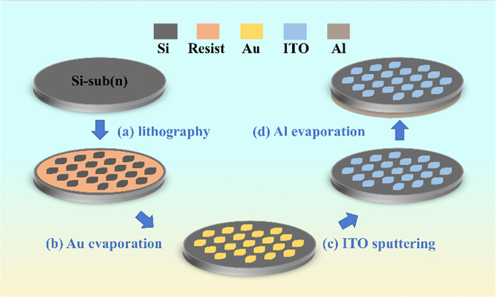
    Schematic process flow for the formation of ITO/Au/n-Si SPDs. (a) The PD areas were defined on an n-type Si substrate by ultraviolet lithography. (b) The patterned Si was sent to the electron beam evaporation chamber to grow Au film at room temperature. (c) 100 nm ITO was deposited on the Au film immediately by a double chamber magnetron sputtering system at room temperature under Ar/O2 atmosphere. (d) The ohmic contact on the backside was realized by a 300 nm Al film using electron beam evaporation.
    Fig. 1. Schematic process flow for the formation of ITO/Au/n-Si SPDs. (a) The PD areas were defined on an n-type Si substrate by ultraviolet lithography. (b) The patterned Si was sent to the electron beam evaporation chamber to grow Au film at room temperature. (c) 100 nm ITO was deposited on the Au film immediately by a double chamber magnetron sputtering system at room temperature under Ar/O2 atmosphere. (d) The ohmic contact on the backside was realized by a 300 nm Al film using electron beam evaporation.
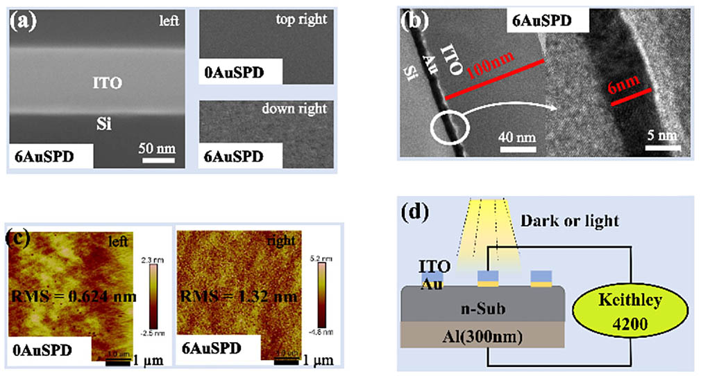
    (a) Cross-sectional scanning electron microscope (SEM) image of the 6AuSPD on the left, and a top view of the SEM images of the 0AuSPD (top) and 6AuSPD (down) in an area of 1 μm×0.5 μm on the right. (b) Cross-sectional high resolution transmission electron microscope (HRTEM) images of the 6AuSPD. (c) Atomic force microscope (AFM) images (scanned area: 5 μm×5 μm) of the 0AuSPD (left) and the 6AuSPD (right). (d) Schematic diagram of the current–voltage measurement for SPDs.
    Fig. 2. (a) Cross-sectional scanning electron microscope (SEM) image of the 6AuSPD on the left, and a top view of the SEM images of the 0AuSPD (top) and 6AuSPD (down) in an area of 1  μm×0.5  μm on the right. (b) Cross-sectional high resolution transmission electron microscope (HRTEM) images of the 6AuSPD. (c) Atomic force microscope (AFM) images (scanned area: 5  μm×5  μm) of the 0AuSPD (left) and the 6AuSPD (right). (d) Schematic diagram of the current–voltage measurement for SPDs.
    (a) Room temperature J–V characteristics on a linear scale for the 0AuSPD and 6AuSPD under dark conditions; the inset map is the corresponding J–V data from −0.2 to 0.4 V. (b) Room temperature J–V characteristics in semi-log for the 0AuSPD and 6AuSPD. (c) Temperature dependent J–V characteristics for the 6AuSPD. (d) In (J/T2) versus 1000/T for the 0AuSPD and 6AuSPD. Experimental photocurrents and dark currents for the 0AuSPD and 6AuSPD with (e) a 1310 nm laser at a power of 1 mW and (f) a 1064 nm laser at a power of 2 mW.
    Fig. 3. (a) Room temperature JV characteristics on a linear scale for the 0AuSPD and 6AuSPD under dark conditions; the inset map is the corresponding JV data from 0.2 to 0.4 V. (b) Room temperature JV characteristics in semi-log for the 0AuSPD and 6AuSPD. (c) Temperature dependent JV characteristics for the 6AuSPD. (d) In (J/T2) versus 1000/T for the 0AuSPD and 6AuSPD. Experimental photocurrents and dark currents for the 0AuSPD and 6AuSPD with (e) a 1310 nm laser at a power of 1 mW and (f) a 1064 nm laser at a power of 2 mW.
    (a) Room temperature J–V characteristics in semi-log for AuSPDs under dark conditions; (b) ln (J/T2) versus 1000/T for AuSPDs. (c) Photoresponse of AuSPDs measured at zero bias voltage from 1100 to 1700 nm. (d) Experimental photocurrents for AuSPDs with 1310 nm wavelength measured from −1 V to 0.3 V. (e) The dark current, photocurrent, and photocurrent-to-dark-current ratio of AuSPDs at a bias of −1 V, 1310 nm, and power of 1 mW.
    Fig. 4. (a) Room temperature JV characteristics in semi-log for AuSPDs under dark conditions; (b) ln (J/T2) versus 1000/T for AuSPDs. (c) Photoresponse of AuSPDs measured at zero bias voltage from 1100 to 1700 nm. (d) Experimental photocurrents for AuSPDs with 1310 nm wavelength measured from 1  V to 0.3 V. (e) The dark current, photocurrent, and photocurrent-to-dark-current ratio of AuSPDs at a bias of 1  V, 1310 nm, and power of 1 mW.
    (a) Samples were measured using a UV-VIS-NIR light spectrophotometer with light normal to the surface. (b) The corresponding photographs of these ITO/Au/glass films were taken under incandescent light with continuous spectrum showing considerable process uniformity in 2 cm×2 cm.
    Fig. 5. (a) Samples were measured using a UV-VIS-NIR light spectrophotometer with light normal to the surface. (b) The corresponding photographs of these ITO/Au/glass films were taken under incandescent light with continuous spectrum showing considerable process uniformity in 2  cm×2  cm.
    Resistivity of ITO/Au films on glass.
    Fig. 6. Resistivity of ITO/Au films on glass.
    (a) AFM images of the top electrodes in the 2AuSPD, 3AuSPD, 4AuSPD, and 6AuSPD with a scanned area of 5 μm × 5 μm. (b) Cross-sectional HRTEM images of the 2AuSPD, 3AuSPD, 4AuSPD, and 6AuSPD.
    Fig. 7. (a) AFM images of the top electrodes in the 2AuSPD, 3AuSPD, 4AuSPD, and 6AuSPD with a scanned area of 5 μm × 5 μm. (b) Cross-sectional HRTEM images of the 2AuSPD, 3AuSPD, 4AuSPD, and 6AuSPD.
    Schematic diagram of the responsivity measurement for the 2AuSPD. A 1310 nm laser with a power of 2 mW was emitted through a single-mode fiber with an inner diameter of 9 μm onto the 2AuSPD arrays. The distance between the detector and the optical fiber outlet was about 2 mm and the numerical aperture (NA) of the fiber was 0.11, leading to a spot with a diameter of 450 μm on the detector.
    Fig. 8. Schematic diagram of the responsivity measurement for the 2AuSPD. A 1310 nm laser with a power of 2 mW was emitted through a single-mode fiber with an inner diameter of 9 μm onto the 2AuSPD arrays. The distance between the detector and the optical fiber outlet was about 2 mm and the numerical aperture (NA) of the fiber was 0.11, leading to a spot with a diameter of 450 μm on the detector.
    Experimental photocurrent for the 2AuSPD with 1310 nm wavelength.
    Fig. 9. Experimental photocurrent for the 2AuSPD with 1310 nm wavelength.
    (a) Responsivity spectra with different biases of all AuSPDs. The values of the responsivities have been calibrated with a 1310 nm laser. (b) External quantum efficiency spectra with different biases of all AuSPDs.
    Fig. 10. (a) Responsivity spectra with different biases of all AuSPDs. The values of the responsivities have been calibrated with a 1310 nm laser. (b) External quantum efficiency spectra with different biases of all AuSPDs.
    Fitting of the photocurrent response curve under 0 V of the AuSPDs.
    Fig. 11. Fitting of the photocurrent response curve under 0 V of the AuSPDs.
    ConfigurationSpecial DesignSBH (eV)Dark Current Density (A/cm2) (at 1  V)Rectification Ratio (at ±1  V)Responsivity (mA/W) (at 1  V)NPDR (mW1) (at 1  V)Refs.
    Au/n-SiSPP/waveguide0.316.057 (ρ15  Ω·cm)13.3 at 1310 nm3.8×102 at 1310 nm[32]
    Au/graphene/p-SiSPP/waveguide0.341.3150 (ρ0.05  Ω·cm)85 at 1550 nm4.25×103 at 1550 nm[33]
    Au/p-SiSPP/grating0.3248.040 (ρ5  Ω·cm)14.5 at 1550 nm0.048 at 1550 nm[34]
    Graphene/p-Si4.5160 (ρ5  Ω·cm)4.6 at 1550 nm (4  V)8.6 at 1550 nm[39]
    Al/p-Si pyramidsSi pyramids0.629.0103 (ρ15  Ω·cm)12 at 1300 nm96 at 1300 nm[40]
    Cu/p-SiWaveguide0.742.2×10550 (lightly doped)0.08 at 1550 nm4.7 at 1550 nm[22]
    NiSi/n-Si0.621.2×105105 (ρ5  Ω·cm)7.4 at 1310 nm7.4×102 at 1310 nm[41]
    ITO/CuO/n-Si0.58.0×10610 (ρ5  Ω·cm)0.0075 at one sun illumination[31]
    ITO/AgNWs/ITO/p-SiNWs0.715.0×105421 (ρ5  Ω·cm)280 at 1310 nm[29]
    ITO/Ag/n-Si0.742.4×1064×105 (ρ0.5  Ω·cm)62 at 1310 nm (0 V)6.2×10⁴ at 1310 nm (0 V)[25]
    Our work0.7953.7×1071.5×108 (ρ0.5  Ω·cm)27 at 1310 nm1.04×105 at 1310 nm
    Table 1. Performance Comparison for Silicon-Based SPDs
    Xinxin Li, Zhen Deng, Jun Li, Yangfeng Li, Linbao Guo, Yang Jiang, Ziguang Ma, Lu Wang, Chunhua Du, Ying Wang, Qingbo Meng, Haiqiang Jia, Wenxin Wang, Wuming Liu, Hong Chen. Hybrid nano-scale Au with ITO structure for a high-performance near-infrared silicon-based photodetector with ultralow dark current[J]. Photonics Research, 2020, 8(11): 1662
    Download Citation