• Photonics Research
  • Vol. 8, Issue 6, 912 (2020)
Pengfei Wang1、2, Guangzhen Luo1、2, Yang Xu3, Yajie Li1、2, Yanmei Su1、2, Jianbin Ma1、2, Ruiting Wang1、2, Zhengxia Yang1、2, Xuliang Zhou1、2, Yejin Zhang1、2, and Jiaoqing Pan1、2、*
Author Affiliations
  • 1Key Laboratory of Semiconductor Materials Science, Institute of Semiconductors, Chinese Academy of Sciences, Beijing 100083, China
  • 2Center of Materials Science and Optoelectronics Engineering, University of Chinese Academy of Sciences, Beijing 100049, China
  • 3Beijing R&D Institute, VanJee Technology, Beijing 100193, China
  • show less
    DOI: 10.1364/PRJ.387376 Cite this Article Set citation alerts
    Pengfei Wang, Guangzhen Luo, Yang Xu, Yajie Li, Yanmei Su, Jianbin Ma, Ruiting Wang, Zhengxia Yang, Xuliang Zhou, Yejin Zhang, Jiaoqing Pan. Design and fabrication of a SiN-Si dual-layer optical phased array chip[J]. Photonics Research, 2020, 8(6): 912 Copy Citation Text show less
    Optical micrograph of the proposed SiN-Si dual-layer optical phased array.
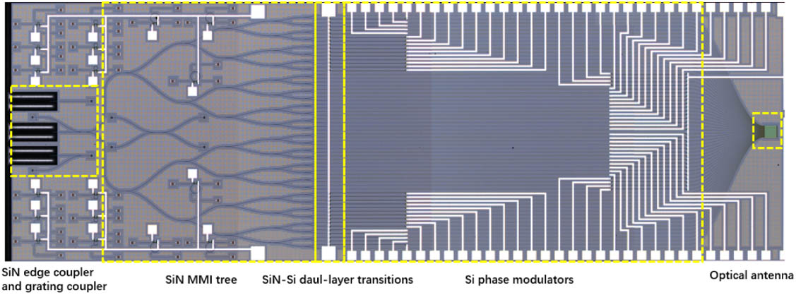
    Fig. 1. Optical micrograph of the proposed SiN-Si dual-layer optical phased array.
    Micrographs of the separate devices: (a) SiN edge coupler, (b) SiN grating coupler, (c) SiN MMI, (d) SiN-Si dual-layer transitions, (e) phase modulators, and (f) optical antenna.
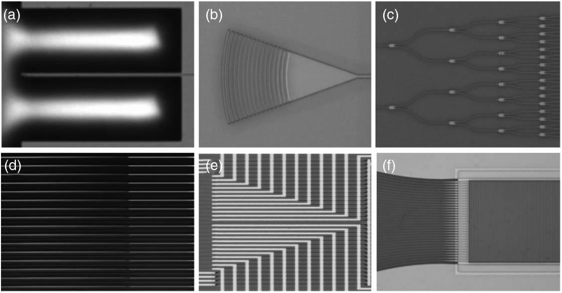
    Fig. 2. Micrographs of the separate devices: (a) SiN edge coupler, (b) SiN grating coupler, (c) SiN MMI, (d) SiN-Si dual-layer transitions, (e) phase modulators, and (f) optical antenna.
    (a) Schematic of the proposed SiN-Si double grating coupler. (b) Sectional view of the proposed SiN-Si double grating coupler. (c) Simulated far-field spot of the proposed SiN-Si double grating coupler. (d) Simulated coupling efficiency of the proposed SiN-Si double grating coupler.
    Fig. 3. (a) Schematic of the proposed SiN-Si double grating coupler. (b) Sectional view of the proposed SiN-Si double grating coupler. (c) Simulated far-field spot of the proposed SiN-Si double grating coupler. (d) Simulated coupling efficiency of the proposed SiN-Si double grating coupler.
    (a) Schematic of the proposed SiN edge coupler. (b) Simulated coupling efficiency of the proposed SiN edge coupler.
    Fig. 4. (a) Schematic of the proposed SiN edge coupler. (b) Simulated coupling efficiency of the proposed SiN edge coupler.
    (a) Schematic of the proposed SiN MMI. (b) Field distribution in the proposed SiN MMI. (c) Simulated transmission efficiency of the proposed SiN MMI.
    Fig. 5. (a) Schematic of the proposed SiN MMI. (b) Field distribution in the proposed SiN MMI. (c) Simulated transmission efficiency of the proposed SiN MMI.
    (a) Schematic of the proposed SiN-Si dual-layer transition. (b) Light intensity transfer between two layers. (c) Optical mode change process at the proposed SiN-Si dual-layer transition. (d) Light transfer efficiency between two layers.
    Fig. 6. (a) Schematic of the proposed SiN-Si dual-layer transition. (b) Light intensity transfer between two layers. (c) Optical mode change process at the proposed SiN-Si dual-layer transition. (d) Light transfer efficiency between two layers.
    (a) Schematic diagram of the thermo-optic phase modulator. (b) Power consumption of phase modulators with different structures.
    Fig. 7. (a) Schematic diagram of the thermo-optic phase modulator. (b) Power consumption of phase modulators with different structures.
    (a) Schematic diagram of the proposed antenna. (b) Scanning far-field spots of the proposed optical antenna.
    Fig. 8. (a) Schematic diagram of the proposed antenna. (b) Scanning far-field spots of the proposed optical antenna.
    (a) Reflection of the antenna. (b) Vector at the beginning of the antenna. (c) Upward and downward emission of the antenna.
    Fig. 9. (a) Reflection of the antenna. (b) Vector at the beginning of the antenna. (c) Upward and downward emission of the antenna.
    (a) Near field and far field with channel1 input light. (b) Near field and far field with channel16 input light. (c) Near field and far field with channel32 input light.
    Fig. 10. (a) Near field and far field with channel1 input light. (b) Near field and far field with channel16 input light. (c) Near field and far field with channel32 input light.
    Test results of the separate devices: (a) loss of the grating coupler, (b) loss of the waveguide, (c) loss of MMI, and (d) loss of SiN-Si dual-layer transition.
    Fig. 11. Test results of the separate devices: (a) loss of the grating coupler, (b) loss of the waveguide, (c) loss of MMI, and (d) loss of SiN-Si dual-layer transition.
    (a) Modulation characteristics of Si thermo-optic phase modulator. (b) Modulation characteristics of SiN thermo-optic phase modulator.
    Fig. 12. (a) Modulation characteristics of Si thermo-optic phase modulator. (b) Modulation characteristics of SiN thermo-optic phase modulator.
    Speed test results of phase modulator.
    Fig. 13. Speed test results of phase modulator.
    (a) Photo of far-field test system and the schematic diagram. (b) Photo of scanning test system and the schematic diagram.
    Fig. 14. (a) Photo of far-field test system and the schematic diagram. (b) Photo of scanning test system and the schematic diagram.
    (a) Beam steering in Φ axis. (b) Beam steering in θ axis. See Visualization 1 for video showing the 2D scanning tested by the far-field test system.
    Fig. 15. (a) Beam steering in Φ axis. (b) Beam steering in θ axis. See Visualization 1 for video showing the 2D scanning tested by the far-field test system.
    (a) Scanning range in Φ axis. (b) Scanning range in θ axis. See Visualization 2 for video showing the 2D scanning tested by the scanning test system.
    Fig. 16. (a) Scanning range in Φ axis. (b) Scanning range in θ axis. See Visualization 2 for video showing the 2D scanning tested by the scanning test system.
    Simulation result of far-field spot size.
    Fig. 17. Simulation result of far-field spot size.
    Output spot power of Si OPA and SiN-Si OPA as a function of input power.
    Fig. 18. Output spot power of Si OPA and SiN-Si OPA as a function of input power.
    Schematic diagram of proportional heating length phase modulators.
    Fig. 19. Schematic diagram of proportional heating length phase modulators.
    Pengfei Wang, Guangzhen Luo, Yang Xu, Yajie Li, Yanmei Su, Jianbin Ma, Ruiting Wang, Zhengxia Yang, Xuliang Zhou, Yejin Zhang, Jiaoqing Pan. Design and fabrication of a SiN-Si dual-layer optical phased array chip[J]. Photonics Research, 2020, 8(6): 912
    Download Citation