• Photonics Research
  • Vol. 8, Issue 6, 912 (2020)
Pengfei Wang1、2, Guangzhen Luo1、2, Yang Xu3, Yajie Li1、2, Yanmei Su1、2, Jianbin Ma1、2, Ruiting Wang1、2, Zhengxia Yang1、2, Xuliang Zhou1、2, Yejin Zhang1、2, and Jiaoqing Pan1、2、*
Author Affiliations
  • 1Key Laboratory of Semiconductor Materials Science, Institute of Semiconductors, Chinese Academy of Sciences, Beijing 100083, China
  • 2Center of Materials Science and Optoelectronics Engineering, University of Chinese Academy of Sciences, Beijing 100049, China
  • 3Beijing R&D Institute, VanJee Technology, Beijing 100193, China
  • show less
    DOI: 10.1364/PRJ.387376 Cite this Article Set citation alerts
    Pengfei Wang, Guangzhen Luo, Yang Xu, Yajie Li, Yanmei Su, Jianbin Ma, Ruiting Wang, Zhengxia Yang, Xuliang Zhou, Yejin Zhang, Jiaoqing Pan. Design and fabrication of a SiN-Si dual-layer optical phased array chip[J]. Photonics Research, 2020, 8(6): 912 Copy Citation Text show less

    Abstract

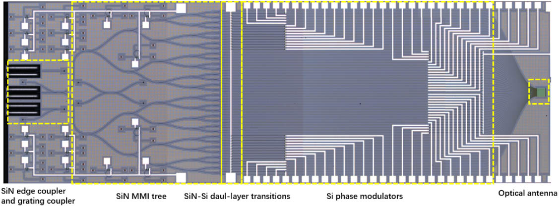
    A SiN-Si dual-layer optical phased array (OPA) chip is designed and fabricated. It combines the low loss of SiN with the excellent modulation performance of Si, which improves the performance of Si single-layer OPA. A novel optical antenna and an improved phase modulation method are also proposed, and a two-dimensional scanning range of 96°×14° is achieved, which makes the OPA chip more practical.
    Δφn,n+1=φn+1φn=nTΔLΔT2πλ,(1)

    View in Article

    ΔL=Ln+1Ln,(2)

    View in Article

    ΔT(ΔU2Rn+1ΔU2Rn),(3)

    View in Article

    ΔT(1Ln+11Ln).(4)

    View in Article

    Δφn,n+1ΔLΔT=(Ln+1Ln)2Ln+1Ln.(5)

    View in Article

    Δφn1,nΔLΔT=(LnLn1)2LnLn1.(6)

    View in Article

    Δφn,n+1=Δφn1,n.(7)

    View in Article

    LnLn1=Ln+1Ln,(8)

    View in Article

    Pengfei Wang, Guangzhen Luo, Yang Xu, Yajie Li, Yanmei Su, Jianbin Ma, Ruiting Wang, Zhengxia Yang, Xuliang Zhou, Yejin Zhang, Jiaoqing Pan. Design and fabrication of a SiN-Si dual-layer optical phased array chip[J]. Photonics Research, 2020, 8(6): 912
    Download Citation