Abstract
A SiN-Si dual-layer optical phased array (OPA) chip is designed and fabricated. It combines the low loss of SiN with the excellent modulation performance of Si, which improves the performance of Si single-layer OPA. A novel optical antenna and an improved phase modulation method are also proposed, and a two-dimensional scanning range of is achieved, which makes the OPA chip more practical.1. INTRODUCTION
With the development of autonomous driving, three-dimensional imaging, remote sensing, and mapping, light detection and ranging (LiDAR) has received great attention. Although there are various LiDAR products on the market [1–5], they do not have advantages in stability and price. These issues make these products unavailable, leading to the need to study new and better LiDAR. The silicon-based optical phased array (OPA) is known as the next generation product due to its low cost, fast speed, and small size. More and more researchers have carried out research on silicon-based OPA and achieved good results [6–21]. For example, in the detection distance, the silicon-based OPA can already detect a distance of 185 m, and the largest OPA has 1024 channels and is integrated with CMOS circuits. These efforts have a very important impetus for the next generation of LiDAR products.
However, silicon-based OPA also has many issues that need to be solved, especially the loss of beam on the chip. Although the processing technology of the silicon-optical platform is relatively stable, there is still a loss of about 3 dB/cm for the optical waveguide, and there are some additional losses, such as coupling loss and transmitting and receiving loss. It is very unfavorable. Moreover, silicon has a strong nonlinear absorption effect, such as two-photon absorption, free carrier absorption, and large lowest order nonlinear effects, which makes the Si single-layer OPA chip unable to handle higher energy light [22]. The best results reported so far also have a total loss of 5–10 dB, which mainly includes coupling loss, spectral loss, and emission loss. If electro-optic phase modulation is used, it will also introduce phase modulation loss, assessed according to the on-chip loss of 10 dB. If the external APD is used to achieve 200 m of detection, an input power of more than 200 mW is required. If the OPA chip is still used for detection, the input power requires about 1 W of input power. This is obviously and extremely disadvantageous for the application of long-range detection. Compared with silicon, silicon nitride (SiN) has lower loss. The thermo-optic coefficient of Si is five times that of SiN, so the power consumption of the Si modulator is lower. Therefore, if the low-loss characteristics of SiN and the good modulation characteristics of Si are combined, it will be a very good solution.
In this paper, we propose a SiN-Si dual-layer OPA chip, which is fabricated on a SiN-on-SOI foundry platform. The SiN is specifically , and the refractive index at the wavelength of 1550 nm is 1.996. The SiN layer is located above the SOI substrate with a spacing of 150 nm silicon dioxide. The silicon devices and the SiN devices are located on two layers and do not interfere with each other. The front-end devices of the OPA chip are some SiN devices, mainly including an input coupler and a cascaded beam splitter, and each device is connected through SiN waveguides. The back-end phase modulators and optical antenna are both silicon devices and are connected through silicon waveguides. The proposed SiN-Si dual-layer OPA chip has excellent low-loss characteristics. Because the front-end devices are made of SiN, the chip can handle very large optical power, providing a basis for long-range detection.
Sign up for Photonics Research TOC. Get the latest issue of Photonics Research delivered right to you!Sign up now
2. STRUCTURE AND CHARACTERISTICS
We have proposed a SiN-Si dual-layer OPA chip, as shown in Fig. 1. The 220 nm top-Si SOI is the substrate, and 400 nm SiN is deposited on it by PECVD with a spacing of 150 nm . The chip mainly consists of five parts, which are the SiN input coupler, SiN multi-mode interference (MMI) tree, SiN-Si dual-layer transitions, Si phase modulators, and optical antenna. The OPA chip combines the respective advantages of two materials, SiN and Si, so that the chip has better performance.
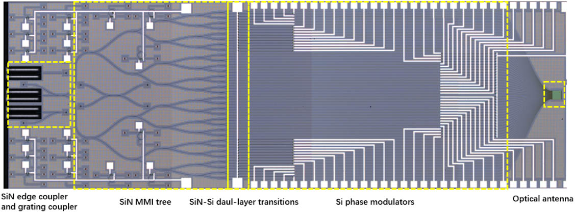
Figure 1.Optical micrograph of the proposed SiN-Si dual-layer optical phased array.
The high-power beam was coupled into the chip through the input coupler, and was divided into several beams by the cascaded MMI. Then the splitted beams were coupled into the silicon waveguides through dual-layer transitions. In this way, the beam arriving in the silicon waveguide has been divided into many parts, and the energy will not be very large, so that it will not suffer from the nonlinear effects of silicon. The beams in the silicon waveguides were then modulated by Si phase modulators, and finally emitted into space through an optical antenna. When the chip is used for receiving, the working principle is similar to that of emission. The signal light is received through the optical antenna, and then modulated by phase modulators. After the cascaded MMI, the beam is detected by the off-chip InGaAs detector or on-chip Ge-Si detector.
The specific structures are shown in Fig. 2. Among them, we provided two types of fiber-chip coupler, edge coupler and grating coupler, which can be selected according to different needs. And the SiN-Si dual-layer transition was designed as a pair of adiabatic linear tapers [22,23]. The beams were transferred from the SiN waveguide to the Si waveguide by means of an evanescent wave. Thermo-optical phase modulators were used, and if the experimental conditions allow, the electro-optic phase modulators will have more excellent performance. The optical antenna is a Si waveguide grating array, but in order to make a larger aperture, a SiN-Si perturbation grating will be adopted in the future [24–26].

Figure 2.Micrographs of the separate devices: (a) SiN edge coupler, (b) SiN grating coupler, (c) SiN MMI, (d) SiN-Si dual-layer transitions, (e) phase modulators, and (f) optical antenna.
In the following, we have simulated each device of the proposed OPA chip.
A. Input Coupler
Because the grating coupler and the edge coupler have their own advantages, we designed these two devices and provided them for the OPA chip together. Among them, the grating coupler has large alignment tolerance, and the package with the fiber is more mature. And the edge coupler has a larger bandwidth, which is very advantageous for the coupling of a multi-wavelength laser.
We have designed a SiN-Si double grating coupler with a structure similar to that in the literature [27]. And we have further optimized the device for our material situation.
As shown in Fig. 3(a), we designed a focusing grating coupler [28]. The coupler has two layers of gratings; one is a SiN grating and one is a Si_slab grating. As shown in Fig. 3(b), the SiN layer is 400 nm thick, the Si_slab layer is 90 nm thick, and the is spaced 150 nm apart. We have optimized our grating parameters according to this material situation. As is known, the loss of the grating coupler mainly comes from two parts; one is the efficiency of the upward coupling of the grating itself, and the other is the mismatch between the intensity distribution of the grating radiation and the mode in the single-mode fiber.
Figure 3.(a) Schematic of the proposed SiN-Si double grating coupler. (b) Sectional view of the proposed SiN-Si double grating coupler. (c) Simulated far-field spot of the proposed SiN-Si double grating coupler. (d) Simulated coupling efficiency of the proposed SiN-Si double grating coupler.
We adopted a double-layered grating structure to reduce light leakage to the substrate, and optimize the grating period and duty cycle to make the light intensity distribution match the mode in the fiber as much as possible. As shown in Fig. 3(c), the proposed grating coupler is coupled to the optical fiber at an angle of 30.6° from the vertical direction. Moreover, as shown in Fig. 3(d), the coupling efficiency of the grating coupler exceeds 78% at 1550 nm, and the 1 dB bandwidth is greater than 100 nm, which has better performance than the ordinary silicon grating coupler.
In addition, we also designed the SiN edge coupler with spot size converter (SSC) structure, as shown in Fig. 4(a). The edge coupler is suspended and consists of a SiN SSC and a cladding. The SiN SSC we designed is 500 μm long and 400 nm thick, and its tip is 300 nm wide. The width and thickness of the coating are both 4 μm, which is to make the light spot on the end face as symmetrical as possible. The tip of SiN SSC is 1 μm away from the end face of the cladding to protect the SSC from damage during the fabrication. We simulated the coupling efficiency of this SiN edge coupler with a single-mode waveguide, and the results are shown in Fig. 4(b). In the 1.5 μm to 1.6 μm wavelength range, the coupling efficiency of the device exceeds 90%.
Figure 4.(a) Schematic of the proposed SiN edge coupler. (b) Simulated coupling efficiency of the proposed SiN edge coupler.
B. SiN MMI
The beam splitters described in the chip are a number of cascaded SiN MMIs, so the performance of each SiN MMI determines the performance of the overall OPA chip. It mainly includes loss and uniformity of light splitting. As shown in Fig. 5(a), we designed a symmetrical , in which the size of the MMI region is , which is connected to the SiN single-mode waveguide through taper structures.
Figure 5.(a) Schematic of the proposed SiN MMI. (b) Field distribution in the proposed SiN MMI. (c) Simulated transmission efficiency of the proposed SiN MMI.
Figure 5(b) shows the light field distribution in the designed SiN MMI. It can be seen that the input beam of light from the left waveguide was evenly divided into two output beams to the right waveguides. Figure 5(c) shows that the loss of the SiN MMI is very small: only about 2% of the light is lost.
C. SiN-Si Dual-Layer Transition
Efficiently coupling the beam in the SiN waveguide into the Si waveguide is a prerequisite for the smooth operation of the proposed OPA chip. We designed a SiN-Si dual-layer transition to achieve this function. The structure of it is shown in Fig. 6(a). It consists of a pair of staggered waveguide tip structures. The SiN waveguide is 900 nm wide and 400 nm thick, with a tip length of 30 μm and a tip width of 300 nm; the silicon waveguide is 450 nm wide and 220 nm thick, and the tip is also 30 μm long and the tip width is 200 nm. The two layers are separated by 150 nm .
Figure 6.(a) Schematic of the proposed SiN-Si dual-layer transition. (b) Light intensity transfer between two layers. (c) Optical mode change process at the proposed SiN-Si dual-layer transition. (d) Light transfer efficiency between two layers.
As shown in Figs. 6(b) and 6(c), the designed SiN-Si dual-layer transition structure can smoothly transfer the beam in the SiN waveguide into the silicon waveguide. Figure 6(d) shows the transition efficiency between the two layers. It can be seen that the beam with a wavelength of 1.5 μm to 1.6 μm can be transferred from the SiN waveguide to the Si waveguide with an efficiency of more than 95%. This enables the weaker beams split from the beam splitters to be successfully transmitted to the phase modulators and optical antenna at the back end.
D. Phase Modulator
We adopted thermo-optic phase modulators to achieve phase adjustment. The specific structure is shown in Fig. 7(a). A high resistivity heating metal, such as TiN, is placed above the waveguide. A voltage is applied to the metal to generate heat, and then heat is transferred into the silicon waveguide to cause phase change. The metal and Si waveguides are separated by to avoid the absorption of light by the metal.
Figure 7.(a) Schematic diagram of the thermo-optic phase modulator. (b) Power consumption of phase modulators with different structures.
We calculated the power consumption of phase modulators with different structures. As shown in Fig. 7(b), the wider the heater, the thicker the spacer layer and the larger the power consumption. We considered the stability of the process and the loss of light. We chose a TiN width of 4 μm and a spacer layer thickness of 2 μm. The lengths of heaters in different channels can be set to different distributions, such as uniform distribution, equal difference distribution, and hyperbolic distribution.
E. Optical Antenna
Optical antennas are adopted to emit beam into space. The usual structure is an arrayed waveguide grating, where the grating period, duty cycle, and etch depth are all related to wavelength. The maximum scanning range of the OPA is related to the pitch of the gratings. In order to avoid crosstalk between waveguides in general optical antennas, the antenna pitch is set to more than one wavelength. For example, if the working wavelength is 1.5 μm to 1.6 μm, the antenna spacing is set to 1.65 μm. However, such a large antenna pitch will severely limit the scanning range of the OPA. We proposed a new optical antenna for this issue. In our previous work, we proposed a new type of optical antenna with a high contrast grating (HCG) structure, which can increase the scanning efficiency while increasing the scanning range [29]. We use a simplified version of this antenna in this paper, adopting a silicon grating on a Si slab to replace the HCG.
The proposed optical antenna is shown in Fig. 8(a), which mainly includes three parts: waveguide array, taper structures, and a grating on a Si slab. The proposed optical antenna is different from general optical antennas. The antenna works as a whole device, and the beams interfere in the Si slab and emit into space through the grating. Therefore, the crosstalk between the antennas need not be considered, and the pitch of the front-end input array waveguide can be quickly increased by bending the waveguide, as shown in Fig. 1. For our optical antenna, the pitch of the input waveguide is set as 1 μm, and it is connected to the back-end Si slab grating by tapers. The length of the taper in front of the designed optical antenna is only 10 μm, and the spacing is quickly increased by bending the waveguide, so the problem of crosstalk is not considered. By changing the phase difference between adjacent input waveguides, we obtained the scanning far-field spot of the OPA chip by simulation. As shown in Fig. 8(b), the proposed optical antenna can achieve a scanning range of more than , which is difficult to achieve for general optical antennas.
Figure 8.(a) Schematic diagram of the proposed antenna. (b) Scanning far-field spots of the proposed optical antenna.
We analyze the reflection of the antenna and the vector at the beginning of the antenna, and the results are shown in Figs. 9(a) and 9(b). For the working band, the reflectivity is less than 7.5%. It can be seen from the vector diagram that the light at the beginning of the antenna is almost not reflected. We also simulated the upward and downward transmittance of the proposed antenna, as shown in Fig. 9(c). The results are shown in the figure below. The upward and downward emission intensity are basically symmetrically distributed, and the upward transmittance is slightly greater than down.
Figure 9.(a) Reflection of the antenna. (b) Vector at the beginning of the antenna. (c) Upward and downward emission of the antenna.
We have analyzed the near and far fields of the input light of a single waveguide in different channels, and the results are shown in Fig. 10. The light transmitted by a single waveguide to a wide grating area will naturally diverge, and the divergent light will have different incidence directions to the antenna’s grating, which will cause the diffracted light spot to form an arc distortion.
Figure 10.(a) Near field and far field with channel1 input light. (b) Near field and far field with channel16 input light. (c) Near field and far field with channel32 input light.
3. TEST RESULTS
A. Device Performance
We performed loss tests on some unit components of the OPA chip, and the results are shown in Fig. 9. First we tested the input grating coupler. By comparing the proposed SiN grating coupler with the general Si grating coupler, we found that the proposed SiN grating coupler has a slightly larger loss, but has a larger 1 dB bandwidth, as shown in Fig. 11(a). The difference between the test results and the simulation results mainly comes from the manufacturing process. We use the 248 Litho process, so the actual structure and design of some devices are biased, especially for grating structures. The SiN grating coupler will be further improved in the future. Because the SiN edge coupler test requires tight horizontal coupling equipment, we have not characterized its characteristics for the time being.
Figure 11.Test results of the separate devices: (a) loss of the grating coupler, (b) loss of the waveguide, (c) loss of MMI, and (d) loss of SiN-Si dual-layer transition.
The waveguide loss is very important for the OPA chip. We measured the Si waveguide and SiN waveguide, and the results are shown in Fig. 11(b). It can be seen that in the 1.5 μm to 1.6 μm band, for most wavelengths, the waveguide loss of SiN is smaller than that of the Si waveguide. The average loss of the Si waveguide is about 2 dB/cm, while the average loss of the SiN waveguide is about 1 dB/cm. So it is very advantageous to introduce the SiN waveguide in an OPA chip.
Then we tested the beam splitter. We compared the performance of the designed SiN MMI with the Si MMI. As shown in Fig. 11(c), the SiN MMI has a smaller loss (0.15 dB) than the Si MMI (0.3 dB). This is beneficial to the overall loss of the OPA chip, because when the OPA scale is large, a very large number of MMIs are required to perform beam splitting.
Then, we characterize the loss of the SiN-Si dual-layer transition, as shown in Fig. 11(d). The loss of the beam through the designed mode converter is about 0.15 dB. It shows that our proposed SiN-Si dual-layer OPA chip can smoothly transfer the light in SiN to a Si waveguide for subsequent processing.
Although the absolute value of the test results of the above devices cannot reach the international best level, introducing SiN devices into OPA chips is a very good solution for the improvement of optical loss and on-chip light intensity.
In addition, we also compared the characteristics of the Si thermo-optic phase modulator and SiN thermo-optic phase modulator, as shown in Figs. 12(a) and 12(b). It can be seen that the power consumption of the silicon phase modulator is relatively small, while the power consumption of the SiN phase modulator is very large. This is mainly because Si has a much larger thermo-optic coefficient than SiN. The maximum phase modulation rate of the thermo-optic phase modulators for Si and SiN is about 15 kHz. Optionally, the phase modulator can also be an electro-optic phase modulator, which will have less power consumption and a faster modulation rate [13].
Figure 12.(a) Modulation characteristics of Si thermo-optic phase modulator. (b) Modulation characteristics of SiN thermo-optic phase modulator.
Regarding the speed of the phase modulator, we tested the rising and falling edges of the MZM. As shown in the Fig. 13, the rise time of the optical response is 4.4 μs, and the fall time is 22.8 μs.
Figure 13.Speed test results of phase modulator.
B. Scanning Performance
We tested the scanning characteristics of the proposed OPA chip. To this end, we built two test systems, as shown in Fig. 14. The system shown in Fig. 14(a) is a far-field test system, and the far-field spot is imaged into an infrared CCD through a set of lenses. This test system can accurately measure the size of the far-field spot, but the scan range that can be measured is small, about . We therefore built a scanning test system, as shown in Fig. 14(b). This test system illuminates the spot emitted by the optical antenna on a screen with an angle ruler, then observes the position of the spot on the screen with an infrared camera, and reads the scanning angle according to the corresponding red calibration light. This test system can test a scanning angle of more than . The angle ruler is a printed screen with an angular grid. The red calibration light directly corresponds to the infrared spot on the screen, and the tester can easily read its scanning angle.
Figure 14.(a) Photo of far-field test system and the schematic diagram. (b) Photo of scanning test system and the schematic diagram.
Through the far-field test system shown in Fig. 14(a), we tested the size and scanning of the emission spot of the OPA chip, and the results are shown in Fig. 15. We use a stochastic gradient descent algorithm to correct and optimize the distorted spot caused by phase errors so that we can quickly get a focused spot. Typically, we test a 32-channel OPA chip. Its far-field spot size is at the wavelength of 1550 nm, and the spot sizes of different wavelengths are slightly different. First, we tested the beam steering in the axis by adjusting the phase gradient. The results are shown in Fig. 15(a). The white dashed line in the figure represents the entire field of view of the test system, and the red dashed line represents the beam steering trajectory. The results show that the far-field spot has been steered, and the actual scanning range is larger than the test range. The steering trajectory of the spot is an arc shape, which is consistent with the simulation results in Fig. 8(b). In combination with wavelength adjustment, the spot steered in the axis, as shown in Fig. 15(b).
Figure 15.(a) Beam steering in axis. (b) Beam steering in axis. See Visualization 1 for video showing the 2D scanning tested by the far-field test system.
We tested the full scan range of our OPA chip through the scanning test system shown in Fig. 14(b). We obtained a scanning range exceeding 96°, as shown in Fig. 16. In addition, when the wavelength changed from 1500 nm to 1580 nm, the spot steered 14°. If the range of the wavelength is larger, the proposed OPA chip will achieve a larger scanning range. Different wavelengths have different interference conditions in the Si_slab layer of the antenna, resulting in different effective apertures, which makes the far-field divergence angles different at different wavelengths.
Figure 16.(a) Scanning range in axis. (b) Scanning range in axis. See Visualization 2 for video showing the 2D scanning tested by the scanning test system.
The spot size we measured at 1550 nm is , and the spot size obtained by simulation is , as shown in Fig. 17. The deviation on the θ axis is mainly that the light spot is obliquely illuminated on the screen or the test optical path, and the measured light spot will be distorted. This problem will be further improved in future tests.
Figure 17.Simulation result of far-field spot size.
We tested the output spot power of SiN-Si OPA and Si OPA as a function of input power, and the results are shown in Fig. 18. Although the SiN-Si OPA chip and Si OPA chip we tested have similar output optical power ( loss) at low input optical power, when the input optical power exceeds 17 dBm, the loss of the Si OPA chip will increase, and the proposed SiN-Si OPA chips do not have this problem. Therefore, SiN-Si OPA chip will be more effective when it needs to detect a longer distance.
Figure 18.Output spot power of Si OPA and SiN-Si OPA as a function of input power.
4. IMPROVEMENTS
We adopted point-by-point optimization of the light spot to characterize the scanning performance of the OPA, which is very inefficient. Although a good optimization algorithm can speed up the optimization rate, if too many points need to be optimized, the workload is still large. We explored a better phase modulator solution that only needs to be optimized once. We use a thermo-optic modulator array of equal proportions; that is, the heating length of each waveguide is proportional. And the premise of adopting this solution is that the antenna spacing is equal.
As shown in Fig. 19, the lengths of the heaters are proportional. The heaters on each waveguide are controlled individually, so designed to calibrate the phase of each channel. When the OPA chip works, first, the far-field spot is focused at a certain angle by adjusting the voltage of each heater. Second, it only needs to increase or decrease the same voltage for all heaters, and the far-field spot will steer continuously.
Figure 19.Schematic diagram of proportional heating length phase modulators.
The specific derivation process is shown below. The phase difference between the ()th channel and the th channel is expressed as where is the coefficient of change of the refractive index with temperature, is the length difference of the heater, is the temperature difference provided by the two heaters, and is the working wavelength. Among them, where is the voltage value changed by each channel, and is the resistance value of the heater. The width and thickness of different heaters are the same—only the length is different—so Eq. (3) can be expressed as Therefore, can be expressed as Similarly, can be expressed as With the same antenna waveguide spacing, in order to achieve beam steering, the following is required: Finally, from Eqs. (5)–(7), we get which is the proportional heating length. The size of the ratio can be set according to the OPA of different scales. If the number of OPA channels is large, the ratio can be set small; otherwise the longest heater will be very long.
5. CONCLUSION
We designed and fabricated a SiN-Si dual-layer OPA chip, which has better low-loss characteristics. The SiN-Si OPA chip we tested has a loss equivalent to that of the Si OPA chip at low input power. But the losses of the SiN waveguide and SiN MMI are smaller than those of silicon; the advantage of low loss will be greater in the case of a larger array. Moreover, SiN-Si OPA chips are not affected by non-linear effects of high-power light. Compared to Si OPA chips, the performance improvement is significant. This work is groundbreaking, which is a boost for the implementation of the OPA-based LiDAR. In addition, we have adopted a brand new optical antenna and tested the scanning characteristics of the antenna. The antenna can achieve a large field of view of more than , and this result is also very leading. In addition, we provided an improved phase modulation method—namely, proportional heaters—to make the OPA work more easily.
Acknowledgment
Acknowledgment. We are very grateful to the Institute of Microelectronics (IME) [30] for completing the chip manufacturing and guaranteeing that the chip can work normally. And we give special thanks to VanJee Technology Co., Ltd. [31] for providing the driver circuit supporting the OPA chip.
References
[1] https://www.velodynelidar.com/. https://www.velodynelidar.com/
[2] https://www.ibeo-as.com/. https://www.ibeo-as.com/
[3] https://innoviz.tech/. https://innoviz.tech/
[4] http://www.leddartech.com/. http://www.leddartech.com/
[5] https://quanergy.com/. https://quanergy.com/
[6] A. Yaacobi, J. Sun, M. Moresco, G. Leake, D. Coolbaugh, M. R. Watts. Integrated phased array for wide-angle beam steering. Opt. Lett., 39, 4575-4578(2014).
[7] J. C. Hulme, J. K. Doylend, M. J. Heck, J. D. Peters, M. L. Davenport, J. T. Bovington, L. A. Coldren, J. E. Bowers. Fully integrated hybrid silicon two dimensional beam scanner. Opt. Express, 23, 5861-5874(2015).
[8] A. Feshali, C. T. Phare, D. N. Hutchison, H. Rong, J. Sun, J. Heck, J. K. Doylend, R. Kumar, W. Kim. High-resolution aliasing-free optical beam steering. Optica, 3, 887-890(2016).
[9] C. V. Poulton, A. Yaacobi, Z. Su, M. J. Byrd, M. R. Watts. Optical phased array with small spot size, high steering range and grouped cascaded phase shifters. Advanced Photonics 2016, IW1B.2(2016).
[10] M. Raval, C. V. Poulton, M. R. Watts. Unidirectional waveguide grating antennas with uniform emission for optical phased arrays. Opt. Lett., 42, 2563-2566(2017).
[11] S. W. Chung, H. Abediasl, H. Hashemi. A monolithically integrated large-scale optical phased array in silicon-on-insulator CMOS. IEEE J. Solid-State Circuits, 53, 275-296(2018).
[12] C. V. Poulton, M. J. Byrd, P. Russo, E. Timurdogan, M. Khandaker, D. Vermeulen, M. R. Watts. Long-range LiDAR and free-space data communication with high-performance optical phased arrays. IEEE J. Sel. Top. Quantum Electron., 25, 7700108(2019).
[13] W. Xie, T. Komljenovic, J. Huang, M. Tran, M. Davenport, A. Torres, P. Pintus, J. Bowers. Heterogeneous silicon photonics sensing for autonomous cars [Invited]. Opt. Express, 27, 3642-3663(2019).
[14] T. Kim. Realization of Integrated Coherent LiDAR(2019).
[15] M. Gehl, G. Hoffman, P. Davids, A. Starbuck, C. Dallo, Z. Barber, E. Kadlec, R. K. Mohan, S. Crouch, C. Long. Phase optimization of a silicon photonic two-dimensional electro-optic phased array. CLEO: Science and Innovations, JTh2A.39(2019).
[16] C. V. Poulton, P. Russo, B. Moss, M. Khandaker, M. J. Byrd, J. Tran, E. Timurdogan, D. Vermeulen, M. R. Watts. Small-form-factor optical phased array module for technology adoption in custom applications. CLEO: Applications and Technology, JTh5B.6(2019).
[17] J. Notaros, M. J. Byrd, M. Raval, M. R. Watts. Integrated optical phased array butterfly architecture for independent amplitude and phase control. Integrated Photonics Research, Silicon and Nanophotonics, IM4A.4(2019).
[18] F. Ashtiani, F. Aflatouni. N × N optical phased array with 2N phase shifters. Opt. Express, 27, 27183-27190(2019).
[19] H. Hashemi. Large-scale monolithic optical phased arrays. Optical Fiber Communication Conference, Tu3E.5(2019).
[20] B. Zhang, N. Dostart, A. Khilo, M. Brand, K. Al Qubaisi, D. Onural, D. Feldkhun, M. A. Popović, K. Wagner. Serpentine optical phased array silicon photonic aperture tile with two-dimensional wavelength beam steering. Optical Fiber Communication Conference, M4E.5(2019).
[21] S.-M. Kim, T.-H. Park, C.-S. Im, S.-S. Lee, T. Kim, M.-C. Oh. Temporal response of polymer waveguide beam scanner with thermo-optic phase-modulator array. Opt. Express, 28, 3768-3778(2020).
[22] W. D. Sacher, Y. Huang, G.-Q. Lo, J. K. Poon. Multilayer silicon nitride-on-silicon integrated photonic platforms and devices. J. Lightwave Technol., 33, 901-910(2015).
[23] Y. Huang, J. Song, X. Luo, T.-Y. Liow, G.-Q. Lo. CMOS compatible monolithic multi-layer Si3N4-on-SOI platform for low-loss high performance silicon photonics dense integration. Opt. Express, 22, 21859-21865(2014).
[24] M. Zadka, Y.-C. Chang, A. Mohanty, C. T. Phare, S. P. Roberts, M. Lipson. On-chip platform for a phased array with minimal beam divergence and wide field-of-view. Opt. Express, 26, 2528-2534(2018).
[25] W. Xie, J. Huang, T. Komljenovic, L. Coldren, J. Bowers. Diffraction limited centimeter scale radiator: metasurface grating antenna for phased array LiDAR(2018).
[26] Y. Zhang, Y.-C. Ling, K. Zhang, C. Gentry, D. Sadighi, G. Whaley, J. Colosimo, P. Suni, S. B. Yoo. Sub-wavelength-pitch silicon-photonic optical phased array for large field-of-regard coherent optical beam steering. Opt. Express, 27, 1929-1940(2019).
[27] W. D. Sacher, Y. Huang, G. Q. Lo, J. K. S. Poon. Multilayer silicon nitride-on-silicon integrated photonic platforms and devices. J. Lightwave Technol., 33, 901-910(2015).
[28] F. Van Laere, T. Claes, J. Schrauwen, S. Scheerlinck, W. Bogaerts, D. Taillaert, L. O’Faolain, D. Van Thourhout, R. Baets. Compact focusing grating couplers for silicon-on-insulator integrated circuits. IEEE Photon. Technol. Lett., 19, 1919-1921(2007).
[29] P. Wang, G. Luo, H. Yu, Y. Li, M. Wang, X. Zhou, W. Chen, Y. Zhang, J. Pan. Improving the performance of optical antenna for optical phased arrays through high-contrast grating structure on SOI substrate. Opt. Express, 27, 2703-2712(2019).
[30] https://www.a-star.edu.sg/ime/. https://www.a-star.edu.sg/ime/
[31] http://www.vanjee.net/. http://www.vanjee.net/


