• Laser & Optoelectronics Progress
  • Vol. 61, Issue 1, 0123002 (2024)
Ruiying Kong1、2, Yijun Wei1、2, Jiacheng Chen1、2, Tianshu Ma1、2, Yaohui Zhan1、2、*, and Xiaofeng Li1、2、**
Author Affiliations
  • 1School of Optoelectronic Science and Engineering, Soochow University, Suzhou 215006, Jiangsu , China
  • 2Key Lab of Advanced Optical Manufacturing Technologies of Jiangsu Province & Key Lab of Modern Optical Technologies of Education Ministry of China, Suzhou 215006, Jiangsu , China
  • show less
    DOI: 10.3788/LOP232375 Cite this Article Set citation alerts
    Ruiying Kong, Yijun Wei, Jiacheng Chen, Tianshu Ma, Yaohui Zhan, Xiaofeng Li. Efficient Photoelectric Coupling Simulation and Machine Learning Study of Perovskite Solar Cells (Invited)[J]. Laser & Optoelectronics Progress, 2024, 61(1): 0123002 Copy Citation Text show less
    Combination of intelligent algorithms such as machine learning and multi-physical field design of photovoltaic devices. Neural networks are not only used for forward prediction (blue circles), but also for reverse design (red circles), achieving a comprehensive design from the material, structure, and other parameters to the photoelectric response
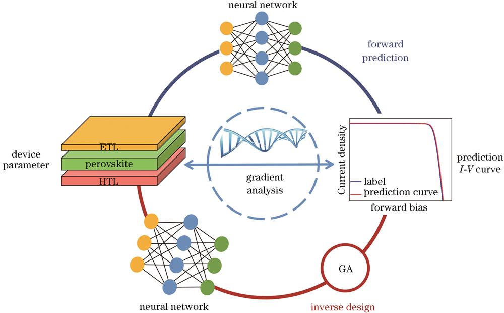
    Fig. 1. Combination of intelligent algorithms such as machine learning and multi-physical field design of photovoltaic devices. Neural networks are not only used for forward prediction (blue circles), but also for reverse design (red circles), achieving a comprehensive design from the material, structure, and other parameters to the photoelectric response
    Structure and energy level diagram of perovskite solar cells. (a) Structural diagram; (b) energy level diagram
    Fig. 2. Structure and energy level diagram of perovskite solar cells. (a) Structural diagram; (b) energy level diagram
    Influence of the parameters such as the thickness of each layer of PSCs on their performance. (a) Absorption contour map within the working band, as the thickness of the perovskite layer changes from 450 nm to 900 nm; (b) plot of the percentage stacking area of absorption and reflection of each layer under illumination; (c) contour map of the macroscopic changes in the current-voltage curve, as the electronic lifetime of the perovskite layer increases from 0.0005 μs to 20 μs; (d) effect of the electronic lifetime of the perovskite layer on the device temperature
    Fig. 3. Influence of the parameters such as the thickness of each layer of PSCs on their performance. (a) Absorption contour map within the working band, as the thickness of the perovskite layer changes from 450 nm to 900 nm; (b) plot of the percentage stacking area of absorption and reflection of each layer under illumination; (c) contour map of the macroscopic changes in the current-voltage curve, as the electronic lifetime of the perovskite layer increases from 0.0005 μs to 20 μs; (d) effect of the electronic lifetime of the perovskite layer on the device temperature
    Machine learning models and their predictive effects. (a) Importance ranking of the input features in the decision tree model; (b) underlying decision tree; (c) cross validation results of 50 random forests; (d) learning curves of the random forests during 200 iteration times
    Fig. 4. Machine learning models and their predictive effects. (a) Importance ranking of the input features in the decision tree model; (b) underlying decision tree; (c) cross validation results of 50 random forests; (d) learning curves of the random forests during 200 iteration times
    Neural network model and its prediction results. (a) Neural network structure diagram; (b) loss value measured by MSE during the training and testing process; (c) comparison between the predicted current-voltage curves and those calculated by the optoelectronic coupling model; (d) comparison of current-voltage curves in the literature and current-voltage curves predicted by machine learning models
    Fig. 5. Neural network model and its prediction results. (a) Neural network structure diagram; (b) loss value measured by MSE during the training and testing process; (c) comparison between the predicted current-voltage curves and those calculated by the optoelectronic coupling model; (d) comparison of current-voltage curves in the literature and current-voltage curves predicted by machine learning models
    Regression results between predicted and true values of four important parameters of perovskite solar cells. (a) Short circuit current; (b) open circuit voltage; (c) fill factor; (d) conversion efficiency
    Fig. 6. Regression results between predicted and true values of four important parameters of perovskite solar cells. (a) Short circuit current; (b) open circuit voltage; (c) fill factor; (d) conversion efficiency
    Comparison between the current-voltage curve fitted by the microscopic parameters of the optimized algorithm design and the actual curve
    Fig. 7. Comparison between the current-voltage curve fitted by the microscopic parameters of the optimized algorithm design and the actual curve
    ParameterSymbolUnitPerovskiteETLHTL
    Electron affinityχeV3.9342.5
    Band gapEgeV1.553.22.7
    Relative permittivityεr6.593
    Effective DOS for electronNCcm-30.23m09m01×1019
    Effective DOS for holeNVcm-30.29m03m01×1019
    Radiative recombination coefficientCcm3·s-13.27×10-1100
    Table 1. Key material parameters for the optoelectronic coupling simulation
    ParameterLayerInputInverse design output
    Thickness /nmGlass9793
    FTO342319
    ETL3439
    Perovskite564572
    HTL153142
    Electron mobilityETL0.4580.452
    Perovskite1.611.81
    HTL0.9850.93
    Electronic lifetime /μsETL0.00050.0005
    Perovskite10.115.76
    HTL0.00750.01
    Doping concentrationETL6.79×10126.83×1012
    Perovskite1.71×10161.99×1016
    HTL6.5×10186.12×1018
    Table 2. Comparison between reverse deduction and true values of five structural parameters and nine electrical parameters
    Ruiying Kong, Yijun Wei, Jiacheng Chen, Tianshu Ma, Yaohui Zhan, Xiaofeng Li. Efficient Photoelectric Coupling Simulation and Machine Learning Study of Perovskite Solar Cells (Invited)[J]. Laser & Optoelectronics Progress, 2024, 61(1): 0123002
    Download Citation