• Journal of Semiconductors
  • Vol. 44, Issue 1, 012001 (2023)
Siwen Zhao1, Gonglei Shao2, Zheng Vitto Han3、4, Song Liu2、*, and Tongyao Zhang3、4、**
Author Affiliations
  • 1Shenyang National Laboratory for Materials Science, Institute of Metal Research, Chinese Academy of Sciences, Shenyang 110010, China
  • 2Institute of Chemical Biology and Nanomedicine, State Key Laboratory of Chemo/Biosensing and Chemometrics, College of Chemistry and Chemical Engineering, Hunan University, Changsha 410082, China
  • 3State Key Laboratory of Quantum Optics and Quantum Optics Devices, Institute of Opto-Electronics, Shanxi University, Taiyuan 030006, China
  • 4Collaborative Innovation Center of Extreme Optics, Shanxi University, Taiyuan 030006, China
  • show less
    DOI: 10.1088/1674-4926/44/1/012001 Cite this Article
    Siwen Zhao, Gonglei Shao, Zheng Vitto Han, Song Liu, Tongyao Zhang. Gate tunable spatial accumulation of valley-spin in chemical vapor deposition grown 40°-twisted bilayer WS2[J]. Journal of Semiconductors, 2023, 44(1): 012001 Copy Citation Text show less
    (Color online) (a) Twisted bilayer WS2 crystal structure and schematic of the band extrema at the K+ and K− points in monolayer WS2. The figure shows the conduction-band and valence-band spin splitting and the allowed optical transitions for circularly polarized light. (b) Schematic of the twisted bilayer WS2 (t-WS2)/h-BN heterojunction device. Optical microscope images of (c) twisted bilayer WS2 transistor on SiO2/Si, (d) t-WS2/h-BN heterostructure, and (e) the final device after lithography patterning. The scale bar is 5μm.
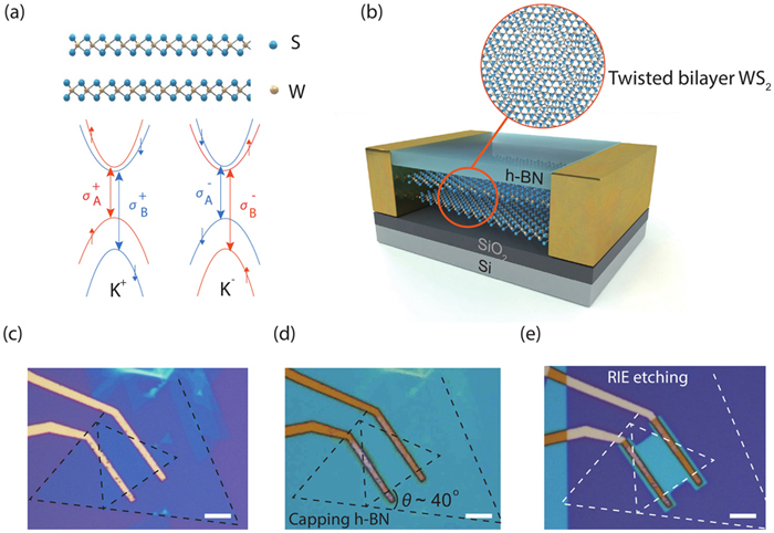
    Fig. 1. (Color online) (a) Twisted bilayer WS2 crystal structure and schematic of the band extrema at the K+ and K points in monolayer WS2. The figure shows the conduction-band and valence-band spin splitting and the allowed optical transitions for circularly polarized light. (b) Schematic of the twisted bilayer WS2 (t-WS2)/h-BN heterojunction device. Optical microscope images of (c) twisted bilayer WS2 transistor on SiO2/Si, (d) t-WS2/h-BN heterostructure, and (e) the final device after lithography patterning. The scale bar is 5μm.
    (Color online) (a) Source–drain current as a function of back-gate voltageVg of the device at 20 K forVds =1 V. (b) PL spectra of the heterostructure at 20 K. In the PL plot, the thick green solid line indicates the measured data, and the red solid line shows the Gaussian fitting result. The four Gaussian components are attributed to the neutral excitons (X0), trions (X-), defect-trapped localized exciton (LX1) or biexciton (XX), and defect-trapped localized exciton (LX2).
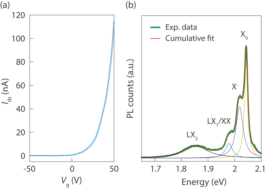
    Fig. 2. (Color online) (a) Source–drain current as a function of back-gate voltageVg of the device at 20 K forVds =1 V. (b) PL spectra of the heterostructure at 20 K. In the PL plot, the thick green solid line indicates the measured data, and the red solid line shows the Gaussian fitting result. The four Gaussian components are attributed to the neutral excitons (X0), trions (X-), defect-trapped localized exciton (LX1) or biexciton (XX), and defect-trapped localized exciton (LX2).
    (Color online) Spatial map of the Kerr rotation angle under (a)Vg = –80 V, (b)Vg = 0 V, and (c)Vg = 20 V. Signals from metal electrodes are not shown as the polarization of reflected light from electrodes is destructed.
    Fig. 3. (Color online) Spatial map of the Kerr rotation angle under (a)Vg = –80 V, (b)Vg = 0 V, and (c)Vg = 20 V. Signals from metal electrodes are not shown as the polarization of reflected light from electrodes is destructed.
    (Color online) Linecuts of the Kerr rotation map under different back gates. Original data and fits are open markers and solid lines, respectively, which are shifted vertically for clarity.
    Fig. 4. (Color online) Linecuts of the Kerr rotation map under different back gates. Original data and fits are open markers and solid lines, respectively, which are shifted vertically for clarity.
    Siwen Zhao, Gonglei Shao, Zheng Vitto Han, Song Liu, Tongyao Zhang. Gate tunable spatial accumulation of valley-spin in chemical vapor deposition grown 40°-twisted bilayer WS2[J]. Journal of Semiconductors, 2023, 44(1): 012001
    Download Citation