1Shenyang National Laboratory for Materials Science, Institute of Metal Research, Chinese Academy of Sciences, Shenyang 110010, China
2Institute of Chemical Biology and Nanomedicine, State Key Laboratory of Chemo/Biosensing and Chemometrics, College of Chemistry and Chemical Engineering, Hunan University, Changsha 410082, China
3State Key Laboratory of Quantum Optics and Quantum Optics Devices, Institute of Opto-Electronics, Shanxi University, Taiyuan 030006, China
4Collaborative Innovation Center of Extreme Optics, Shanxi University, Taiyuan 030006, China
The emerging two-dimensional materials, particularly transition metal dichalcogenides (TMDs), are known to exhibit valley degree of freedom with long valley lifetime, which hold great promises in the implementation of valleytronic devices. Especially, light–valley interactions have attracted attentions in these systems, as the electrical generation of valley magnetization can be readily achieved — a rather different route toward magnetoelectric (ME) effect as compared to that from conventional electron spins. However, so far, the moiré patterns constructed with twisted bilayer TMDs remain largely unexplored in regard of their valley spin polarizations, even though the symmetry might be distinct from the AB stacked bilayer TMDs. Here, we study the valley Hall effect (VHE) in 40°-twisted chemical vapor deposition (CVD) grown WS2 moiré transistors, using optical Kerr rotation measurements at 20 K. We observe a clear gate tunable spatial distribution of the valley carrier imbalance induced by the VHE when a current is exerted in the system.The emerging two-dimensional materials, particularly transition metal dichalcogenides (TMDs), are known to exhibit valley degree of freedom with long valley lifetime, which hold great promises in the implementation of valleytronic devices. Especially, light–valley interactions have attracted attentions in these systems, as the electrical generation of valley magnetization can be readily achieved — a rather different route toward magnetoelectric (ME) effect as compared to that from conventional electron spins. However, so far, the moiré patterns constructed with twisted bilayer TMDs remain largely unexplored in regard of their valley spin polarizations, even though the symmetry might be distinct from the AB stacked bilayer TMDs. Here, we study the valley Hall effect (VHE) in 40°-twisted chemical vapor deposition (CVD) grown WS2 moiré transistors, using optical Kerr rotation measurements at 20 K. We observe a clear gate tunable spatial distribution of the valley carrier imbalance induced by the VHE when a current is exerted in the system.
Introduction
Manipulating the valley degree of freedom in TMDs has aroused tremendous interests recently due to the large enough energy degeneracy lifting by spin-orbit coupling (SOC) in them[1-5]. Valley Hall is a representative effect that can be probed by either transport or optical measurements due to the chiral nature of the propagation of the valley pseudo-spins[6,7]. Even though monolayer TMDs are believed to exhibit rather weak valley Hall signals, studies revealed that electrical control of valley magnetizations are detectable by Kerr rotation microscopy in such as n- or p-doped monolayer WSe2, and also in single-layer MoS2 under a uniaxial stress with broken rotational symmetry[8,9]. It thus makes the TMD materials very promising for future designing of valleytronic devices incorporated with light-matter interactions[10].
AB stacked bilayer systems such as MoS2 offer broken inversion symmetry that arises from the vertical electric field induced by electrostatic gating. It hence leads to a pronounced valley polarization effect that gathers ‘magnetized’ valley at the sample edge in the existence of a finite longitudinal electrical current[6]. Indeed, by using Kerr rotation microscopy, such polarization was found to be present only near the edges of the device channel with opposite sign for the two edges, and was out-of-plane and strongly dependent on the gate voltage in AB-stacked bilayer MoS2, similar to that observed in the spin Hall effect manifested in conventional thin magnetic or antiferromagnetic films with large SOC[11,12]. This behavior is also believed to be consistent with symmetry-dependent Berry curvature and valley Hall conductivity in bilayer MoS2[6].
Nevertheless, a twisted bilayer of TMD, which yields a variety of fundamental physics including flat bands and strong e–e interactions[13,14], have been overlooked thus far in regard to the investigation of valley Hall effect in them. Especially, when constructed with a certain twist angle, the symmetry breaking spontaneously takes place, which should be more favorable in terms of the detection of valley degree of freedom in those moiré systems[15].
Here, we show the study of the valley Hall effect (VHE) in 40°-twisted chemical vapor deposition (CVD) grown WS2 moiré transistors, using optical Kerr rotation measurements at 20 K. We observe a clear gate tunable spatial distribution of the valley carrier imbalance induced by the VHE when a current is exerted in the system. Further, our results demonstrate that TMD moiré heterostructure can offer an attractive platform for probing and manipulating valley degree of freedom.
The fabrication of 40°-twisted bilayer WS2 transistors
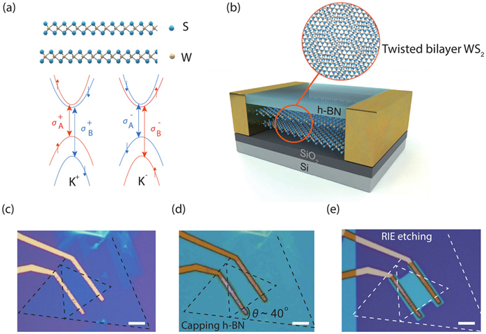
To fabricate the WS2 moiré transistors, the twisted bilayer WS2 with different angles were first grown on the SiO2/Si substrates by an improved CVD method with the assistance of heteroatom tin (Sn) for reducing stacking energy. The details of the process of growth can be found in our former article[16]. Systematic characterizations using optical spectroscopy of the studied devices are carried out, with the details shown in Supplementary Fig. S1. To further confirm local atomic configuration and interlayer stacking induced moiré superlattice, scanning transmission electron microscopy (STEM) characterization of typical twisted WS2 double layers (0° and 40° twisted, for example) are shown in Supplementary Fig. S2.Fig. 1(a) shows the schematic of twisted bilayer WS2 and the spin-split conduction band minima and valence band maxima near the K+ and K− valleys. The spin and valley degree of freedom can be selectively operated using circularly polarized light due to the optical selection rule[17,18]. Thus, with linearly polarized light, we can probe the accumulation of spin-polarized and valley-polarized carriers using the measurement of magneto-optic Kerr rotation (KR)[19]. The signal of Kerr rotation should be opposite for the K+ and K− valleys due to the opposite sign of the Berry curvature around the two valleys. To obtain a better sample quality and enhance the mobility of WS2, we transferred multi-layered h-BN flakes onto the top of twisted bilayer WS2. The van der Waals heterostructures were then shaped into rectangular geometry by using standard electron-beam lithography and dry etching in a plasma system. The edge contact electrodes (5 nm Cr/50 nm Au) to WS2 were deposited by electron-beam evaporation. The corresponding optical images of a typical device for every step are shownFigs. 1(c)–1(e). For this device, the twist angle of the as-grown bilayer WS2 is about 40°.Fig. 1(b) shows a schematic of the final device structure.
Figure 1.(Color online) (a) Twisted bilayer WS2 crystal structure and schematic of the band extrema at the K+ and K− points in monolayer WS2. The figure shows the conduction-band and valence-band spin splitting and the allowed optical transitions for circularly polarized light. (b) Schematic of the twisted bilayer WS2 (t-WS2)/h-BN heterojunction device. Optical microscope images of (c) twisted bilayer WS2 transistor on SiO2/Si, (d) t-WS2/h-BN heterostructure, and (e) the final device after lithography patterning. The scale bar is 5μm.
In the following, we show the electrical and optical properties of the t-WS2 field effect transistor, being mounted in a close-cycle Montana Instrument cryostat. The transfer curves of the device forVds = 1 V at 20 K is presented inFig. 2(a), which clearly shows good n-type behavior of WS2. With the help of the capping h-BN on t-WS2, the hysteresis in the transfer curves is not remarkable.Fig. 2(b) shows the PL spectra of t-WS2 at 20 K. The moiré transistor is excited by a 532 nm continuous-wave laser with a spot size of ~1µm focused by a high numerical objective. To obtain better signal-to-noise ratio, the excitation power is kept 300µW. From the PL spectra confocally collected by a monochromator and detected by a CCD camera, we can see four evident peaks. Experimental PL data are compared with simulations allowing the deconvolution of the PL spectra. The detailed fitting for different contributions is shown inFig. 2(b). In previous reports, the two distinguished peaks of high energies at about 2.02 and 2.04 eV were attributed to neutral exciton (X0) and trion (X−), respectively[20]. The trions observed in our experiments indicate intrinsic doping of the as-grown t-WS2 flakes, as it is commonly observed in other TMDs grown by CVD[21]. Apart from the peaks of exciton and trion, a very broad peak shows up around 1.85 eV. This broad peak can be recognized as the defect-trapped localized exciton (LX2) emission and the broad bandwidth arises from the interaction between defect-trapped excitons and phonons[22-25]. Note that the trion peak X− develops a low-energy shoulder located ~ 1.97 eV. This new peak may possibly stems from defect-trapped localized exciton (LX1) and biexciton (XX), which is beyond our scope of this paper[20].
Figure 2.(Color online) (a) Source–drain current as a function of back-gate voltageVg of the device at 20 K forVds =1 V. (b) PL spectra of the heterostructure at 20 K. In the PL plot, the thick green solid line indicates the measured data, and the red solid line shows the Gaussian fitting result. The four Gaussian components are attributed to the neutral excitons (X0), trions (X-), defect-trapped localized exciton (LX1) or biexciton (XX), and defect-trapped localized exciton (LX2).
Gate tunable spatial accumulation of valley spins in the devices
In the following part, we will study the emerging valley Hall effect in our t-WS2 device. Spatially resolved magneto-optic KR is implemented to measure the microscopic spin-valley accumulation in real space. An ACVds = 2 V RMS is exerted to the device to generate oscillating longitudinal charge current. The out-of-plane spin-valley polarization is probed by a linearly polarized laser with photon energy optimized to the lower energy side of X0. The reflected probe laser is analyzed by a polarization sensitive photoreceiver system. To mitigate possible heating effects, the optical power of probe laser is selected to 10µW. To further determine the spatial distribution and magnitude of the spin accumulation, the 2D lateral distribution of the KR is mapped by an electrically-driven X-Y scanner.Fig. 3 shows the KR map of the t-WS2 device at different gate voltages. The magnitude of KR signals atVg = –80 V have little change and the sign is the same across the channel, as shown in yellow squares ofFig. 4. This overall positive KR probably arises from the magnetoelectric effect induced by the strain in the sample[9]. However, whenVg varies from 0 to 20 V, we can clearly see that the sign of KR is opposite on the two edges across the channel, which is resulted from the accumulation of carriers with opposite valley and spin. Note that the offset of the KR peaks atVg = 0 V and 20 V is almost the same, suggesting the saturation of the accumulated carriers atVg = 0 V.
Figure 3.(Color online) Spatial map of the Kerr rotation angle under (a)Vg = –80 V, (b)Vg = 0 V, and (c)Vg = 20 V. Signals from metal electrodes are not shown as the polarization of reflected light from electrodes is destructed.
Figure 4.(Color online) Linecuts of the Kerr rotation map under different back gates. Original data and fits are open markers and solid lines, respectively, which are shifted vertically for clarity.
To analyze the KR maps more quantitively, we linecut the KR maps orthogonal to the electrical current direction, as depicted with dashed lines inFig. 3. The linecut data are plotted inFig. 4. We consider a diffusion-drift model to describe the spin accumulation at channel edge phenomenologically. And the net spin-valley distribution perpendicular to the direction of charge transport can be simply solved in
wherelD is the spin-valley diffusion length,y1 +y2 is the width of the channel[8]. As mentioned above, the KR forVg = –80 V remains unchanged across the transverse channel because of the lack of charge conductance of the n-type transistor. However,lD are ~ 500 nm fit by Eq. (1) forVg = 0 V andVg = 20 V respectively (solid lines inFig. 4), indicating that KR distribution are almost the same in the regime of electron doping. It’s quite counterintuitive as KR is supposed to be linear with charge current density for a certain device with constant spin Hall angle, butIds increases 3 times fromVg = 0 to 20 V fromFig. 2(a). We also note that the spin-valleys are maximized inside the channel, around 3µm far from the edge. It may be understood by some defect-induced scattering centers that prevent the complete separation of carriers with K+ and K-.
Conclusion
In conclusion, we have firstly observed the gate-tunable valley Hall effect in twisted bilayer WS2 transistor by measuring the spatial distribution of the KR induced by spin and valley imbalance. It seems that the CVD twisted bilayer WS2 suffers from strains and/or defects, and the moiré superlattice played limited role in the valley Hall effect. Future studies in cleaner samples, and smaller twist angles will be needed. Our findings provide new insights into electrical control of the valley Hall effect in twisted bilayer TMDs and open up new possibilities for the study of spin and valley properties in moiré superlattice.
Acknowledgements
This work is supported by the National Key R&D Program of China (No. 2019YFA0307800). The work gratefully acknowledges financial support from the National Natural Science Foundation of China (Nos. 22175060, 21975067, 92265203, 11974357, 12004259, 12204287, U1932151), Natural Science Foundation of Hunan Province of China (Nos. 2021JJ10014, 2021JJ30092), and China Postdoctoral Science Foundation (Grant No. 2022M723215).