
Quanxin Yang, Hongliang Liu, Shan He, Qingyu Tian, Bin Xu, Pengfei Wu. Circular cladding waveguides in Pr:YAG fabricated by femtosecond laser inscription: Raman, luminescence properties and guiding performance[J]. Opto-Electronic Advances, 2021, 4(2): 200005-1
- Opto-Electronic Advances
- Vol. 4, Issue 2, 200005-1 (2021)
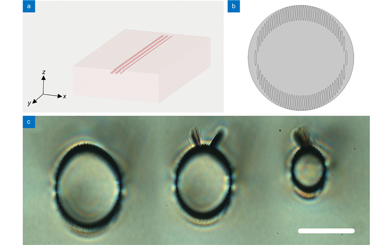
Fig. 1. (a ) The 3D schematic diagram of waveguides. Coordinate axes are defined. (b ) The 2D geometry structure (corresponding to the 120 μm waveguide), which is also used in the guiding mode simulation process. (c ) The cross-section microscope images of the circular cladding waveguides with different diameters: 120 μm, 100 μm, and 60 μm, respectively. The scale bar in the figure is 100 μm.
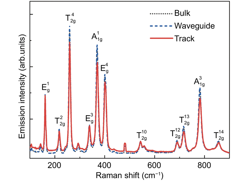
Fig. 2. Raman spectra collected from non-processed bulk area (black dotted line, covered by almost identical blue dashed line), waveguide volume (blue dashed line), and damage track (red solid line) excited by a 532 nm laser . Corresponding molecular vibration modes are marked out on every peak.
Fig. 3. C onfocal μ-Raman 2D mapping results are exhibited as 2D and 3D images with imaging channels. a ) and (d ) Intensity (normalized); (b ) and (e ) Shift; (c ) and (f ) FWHM of the characteristic peak at 259 cm-1, respectively. The scale bar in the figure is 20 μm.
Fig. 4. Luminescence emission spectra of waveguide volume (blue dashed line) and non-processed bulk area (red solid line). Inset shows the output end-face image captured by a color CCD camera while a laser beam at 400 nm has been coupled into the waveguide through another end-face.
Fig. 5. A specific kind of modes with an intensity distribution of horizontal fringes in waveguides with different diameters. (a ) and (d ) 120 μm; (b ) and (e ) 100 μm; (c ) and (f ) 60 μm. (a−c) Experimental mode intensity distributions gained by the end-face coupling system using a laser beam at 632.8 nm. (d−f) Corresponding simulation results. The effective refractive indexes are 1.8392, 1.8390 and 1.8389, respectively. Red arrows point to the directions of electric field. The scale bar in the figure is 20 μm.
Fig. 6. Simulated mode profiles and corresponding horizontally polarized electric field distributions of (a ) and (c ) the circularly symmetric fiber model; (b ) and (d ) the elliptical fiber model. The effective refractive indexes are 1.8395 and 1.8394, respectively. Red arrows point to the directions of electric field.
|
Table 1. The losses of the fabricated cladding waveguides in Pr:YAG at 632.8 nm.


Set citation alerts for the article
Please enter your email address

© Copyright 2018-2021 | Chinese Laser Press. All Rights Reserved 沪ICP备15018463号-20