• Laser & Optoelectronics Progress
  • Vol. 59, Issue 3, 0300003 (2022)
Lili Zhang1、2, Shufeng Sun1、2、*, Xi Wang1、2, Fengyun Zhang1、2, Pingping Wang2, Chengming Cao3、4, and Zibin Zhang5
Author Affiliations
  • 1School of Mechanical and Automotive Engineering, Qingdao University of Technology, Qingdao , Shandong 266520, China
  • 2Shandong Research Center of Laser Green and High Efficiency Intelligent Manufacturing Engineering Technology, Qingdao , Shandong 266520, China
  • 3School of Mechanical and Electrical Engineering, China University of Mining and Technology, Xuzhou , Jiangsu 221116, China
  • 4Shandong Energy Heavy Industry Group Hengtu Technology Co., Ltd., Taian, Shandong 271222, China
  • 5Qingdao Gocci Opto-Electronics Technology Co., Ltd., Qingdao , Shandong 266109, China
  • show less
    DOI: 10.3788/LOP202259.0300003 Cite this Article Set citation alerts
    Lili Zhang, Shufeng Sun, Xi Wang, Fengyun Zhang, Pingping Wang, Chengming Cao, Zibin Zhang. Research Progress of Laser Micro-Nano Connection Technology[J]. Laser & Optoelectronics Progress, 2022, 59(3): 0300003 Copy Citation Text show less
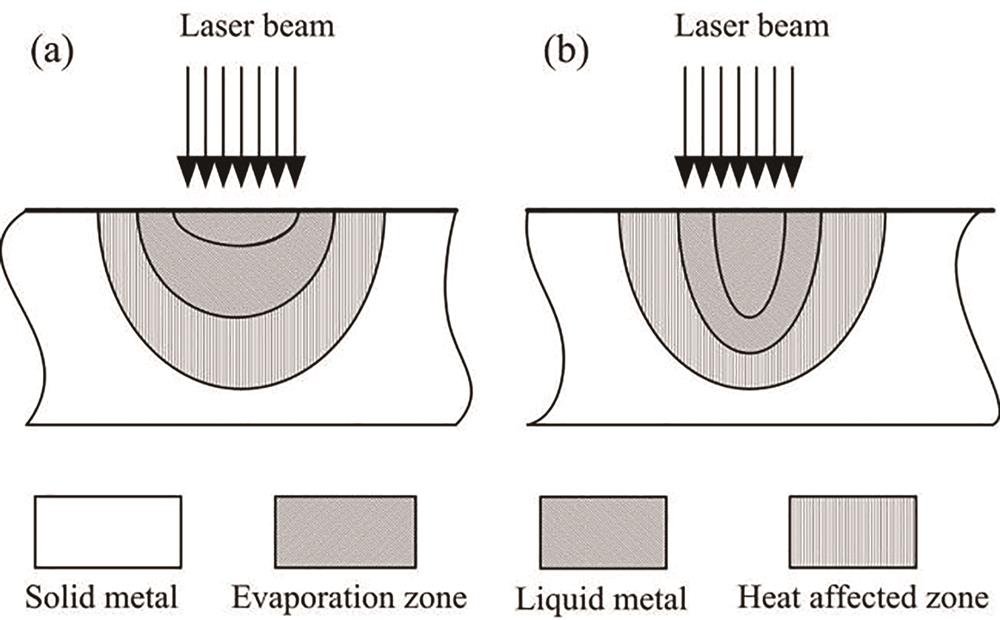
    Different welding modes in laser micro welding[18]. (a) Heat conduction welding; (b) deep penetration welding
    Fig. 1. Different welding modes in laser micro welding[18]. (a) Heat conduction welding; (b) deep penetration welding
    Variation of penetration depth in laser micro welding with laser power and welding speed[19-20]
    Fig. 2. Variation of penetration depth in laser micro welding with laser power and welding speed[19-20]
    Influence of different processing environments on weld morphology under laser micro welding. (a) Morphology of weld under with and without shielding gas[27]; (b) weld morphology under different pressure[28]
    Fig. 3. Influence of different processing environments on weld morphology under laser micro welding. (a) Morphology of weld under with and without shielding gas[27]; (b) weld morphology under different pressure[28]
    Weld morphology of different scanning methods under laser micro welding[32]. (a)‒(c) Circumcision scan; (d)‒(f) linear scan
    Fig. 4. Weld morphology of different scanning methods under laser micro welding[32]. (a)‒(c) Circumcision scan; (d)‒(f) linear scan
    Weld morphology under different defocusing amount under laser micro welding[33]. (a) Weld morphology in positive defocusing state; (b) weld morphology in negative defocus state
    Fig. 5. Weld morphology under different defocusing amount under laser micro welding[33]. (a) Weld morphology in positive defocusing state; (b) weld morphology in negative defocus state
    Welding morphology of laser micro-welded NiTi SMA[38]
    Fig. 6. Welding morphology of laser micro-welded NiTi SMA[38]
    Microscopic images of laser micro-welded nanostructures[40-41]. (a) Laser micro welding of gold nanoparticles; (b) laser micro welding nano-tip
    Fig. 7. Microscopic images of laser micro-welded nanostructures[40-41]. (a) Laser micro welding of gold nanoparticles; (b) laser micro welding nano-tip
    Applications of laser micro welding technology in transparent materials[50-51]
    Fig. 8. Applications of laser micro welding technology in transparent materials[50-51]
    Schematic of laser soldering technology[54]
    Fig. 9. Schematic of laser soldering technology[54]
    Influence of laser power and welding time on solder spread area under laser soldering[56]
    Fig. 10. Influence of laser power and welding time on solder spread area under laser soldering[56]
    Influence of welding speed on welding strength under laser soldering[59]
    Fig. 11. Influence of welding speed on welding strength under laser soldering[59]
    Laser soldering of QFP devices[65]. (a) Finite element simulation welding temperature field model; (b) welding effect diagram of laser soldering technology
    Fig. 12. Laser soldering of QFP devices[65]. (a) Finite element simulation welding temperature field model; (b) welding effect diagram of laser soldering technology
    Microstructure morphology of solder joints under different processing methods[69]. (a) Infrared reflow welding; (b) diode-laser soldering
    Fig. 13. Microstructure morphology of solder joints under different processing methods[69]. (a) Infrared reflow welding; (b) diode-laser soldering
    Application of laser soldering in lead-free solder[76]
    Fig. 14. Application of laser soldering in lead-free solder[76]
    Influence of different content of Zn in SnAgCu solder on soldering strength[82]
    Fig. 15. Influence of different content of Zn in SnAgCu solder on soldering strength[82]
    Sectional view of cable connection device[85]. (a) Laser soldering cable device; (b) microstructure diagram of solder paste and metal connection
    Fig. 16. Sectional view of cable connection device[85]. (a) Laser soldering cable device; (b) microstructure diagram of solder paste and metal connection
    Principle of laser soldering bumping technology[86]
    Fig. 17. Principle of laser soldering bumping technology[86]
    Changes of solder ball morphology under different parameters during laser soldering bumping[91]. (a) Pit defect; (b) offset defect; (c) ablation defect; (d) qualified appearance
    Fig. 18. Changes of solder ball morphology under different parameters during laser soldering bumping[91]. (a) Pit defect; (b) offset defect; (c) ablation defect; (d) qualified appearance
    Two different scanning methods[95]. (a) Cross scan method; (b) linear scanning method
    Fig. 19. Two different scanning methods[95]. (a) Cross scan method; (b) linear scanning method
    Connection typeMacro connectionsSubmilli connectionMicro connectionSubmicron connectionNano connection
    Dimension range≥1 mm0.5‒1 mm1‒500 μm0.1‒1 μm1‒100 nm
    Table 1. Joining categories based on size of connected materials[15]
    Lili Zhang, Shufeng Sun, Xi Wang, Fengyun Zhang, Pingping Wang, Chengming Cao, Zibin Zhang. Research Progress of Laser Micro-Nano Connection Technology[J]. Laser & Optoelectronics Progress, 2022, 59(3): 0300003
    Download Citation