
Jung-Hong Min, Kwangjae Lee, Tae-Hoon Chung, Jung-Wook Min, Kuang-Hui Li, Chun Hong Kang, Hoe-Min Kwak, Tae-Hyeon Kim, Youyou Yuan, Kyoung-Kook Kim, Dong-Seon Lee, Tien Khee Ng, Boon S. Ooi. Large-scale and high-quality III-nitride membranes through microcavity-assisted crack propagation by engineering tensile-stressed Ni layers[J]. Opto-Electronic Science, 2022, 1(10): 220016
- Opto-Electronic Science
- Vol. 1, Issue 10, 220016 (2022)
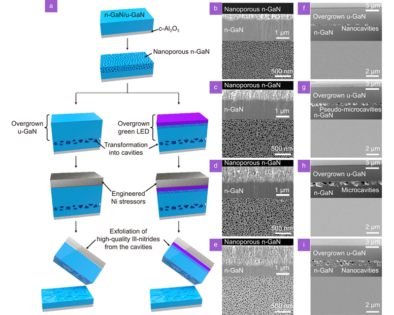
Fig. 1. (a ) A summary of the schematic illustration for the exfoliation of large-scale and high-quality III-nitride layers through microcavity-assisted crack propagation to achieve membrane-based applications such as surface-emitting vertical-type green LEDs (V-LEDs), as well as surface-absorbing vertical-type ultraviolet photodetectors (V-UV PDs). (b –e ) Scanning electron microscope (SEM) images of cross-sectional and top views for the nanoporous n-GaN layers manufactured by various EC etching conditions: 15 V for 5 min (b), 10 min (c ), and 15 min (d ) by using heavily doped n-GaN, and 20 V for 15 min (e) by using lightly doped n-GaN. In order, each nanoporous n-GaN is designated as ‘Nanoporous 1’, ‘Nanoporous 2’, ‘Nanoporous 3’, and ‘Nanoporous 4’. The porosity and depth of the nanoporous structures can be varied through the input voltage, time, and doping concentration. (f –i ) Focused ion beam (FIB)-SEM and SEM images of cross-sectional and top views for the overgrown u-GaN layers. The overgrown u-GaN layers on the nanoporous structures are named ‘Overgrown u-GaN 1’, ‘Overgrown u-GaN 2’, ‘Overgrown u-GaN 3’, and ‘Overgrown u-GaN 4’. After overgrowing the u-GaN layers, cavities were formed with different shapes and sizes according to the original nanoporous structures.
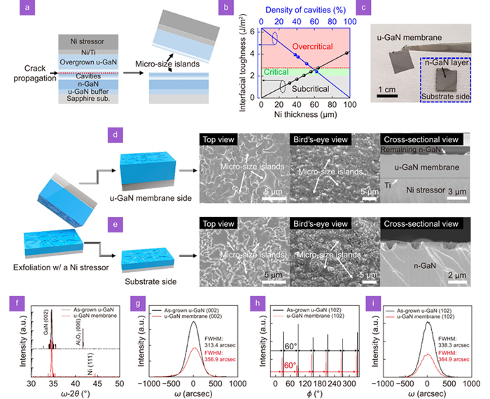
Fig. 2. (a ) A representative schematic illustration of microcavity-assisted crack propagation. (b ) The values of the interfacial toughness of GaN depending on the density of the cavities (blue-colored line) and the applied interfacial toughness through the Ni stressors (black-colored line). The maximum value of the interfacial toughness is 6.38 J/m2 with reference to GaN (002). The blue- and black-colored spheres are the experimental data points obtained from the estimated cavity densities and Ni stressors, respectively. (c ) A digital camera image of a u-GaN membrane acquired from ‘Overgrown u-GaN 3’ after successful exfoliation with the well-engineered Ni stressor. The inset shows the substrate side after exfoliation. (d –e ) Representative schematic illustrations for the u-GaN membrane side and the substrate side and the related SEM and FIB-SEM images for the top, bird’s eye, and cross-sectional views, respectively. The microsized islands were observed on the surface of the membrane and the substrate after exfoliation. (f –i ) Results of the various XRD measurements to check the quality of the u-GaN membrane after exfoliation: ω-2θ scan (f), ω rocking curve for (002) orientations (g ), ϕ scan for (102) orientations (h ), and ω rocking curve for (102) orientations (i).
Fig. 3. (a ) SEM images of the top and cross-sectional views for an overgrown green LED on ‘Nanoporous 2’. The blue-colored dash indicates the detailed top-most areas of the green LED through a high-angle annular dark-field scanning transmission electron microscope (STEM) image and the related STEM-energy dispersive X-ray analysis mapping. (b ) A digital camera image of a green LED membrane exfoliated from cavities with a well-engineered Ni stressor. The inset shows the substrate side after exfoliation. (c ) Results of photoluminescence of the green LED before and after exfoliation. The 473 nm Cobolt laser was used for the as-grown green LED and the green LED membrane due to the peak wavelength of the green LED (~533 nm), and the He-Cd 325 nm laser was employed for the substrate side. (d -e ) Representative schematic illustrations for the green LED membrane side and the substrate side and the related SEM and FIB-SEM images for the top, bird’s eye, and cross-sectional views, respectively. Wider microsized islands were observed on the surfaces of the membrane and the substrate compared to the u-GaN membrane.
Fig. 4. Device applications using green LEDs and u-GaN membranes. (a –b ) Current density-voltage and electroluminescence (EL) spectral characteristics of the V-LEDs. The peak wavelength of the V-LEDs was ~525 nm. (c ) Optical microscope EL images of the green V-LEDs according to input voltages. (d ) Current–voltage characteristics of the V-UV PDs under illumination at 360 nm (0.53 mW/cm2). (e ) Responsivity of the V-UV PDs at –5 V according to wavelengths from 300 nm to 440 nm. The peak responsivity was 8.78 A/W at 360 nm, and the responsivity spectrum showed a high selectivity of the wavelength over 350−370 nm. (f ) Measured values of the current density depending on the illuminated light intensity from 1.39 × 10⁻³ to 6.71 mW/cm2 at –5 V. (g ) Time response characteristics measured by using a 375 nm laser diode at –5 V. The UV laser pulses were 1 kHz. (h -i ) The zoom-in time response curve and its biexponential fitting curves to obtain the rise time and decay time. The rise and decay times are 145 and 205 μs, respectively.

Set citation alerts for the article
Please enter your email address
© Copyright 2018-2021 | Chinese Laser Press. All Rights Reserved 沪ICP备15018463号-20