Abstract
![]()
Epitaxially grown III-nitride alloys are tightly bonded materials with mixed covalent-ionic bonds. This tight bonding presents tremendous challenges in developing III-nitride membranes, even though semiconductor membranes can provide numerous advantages by removing thick, inflexible, and costly substrates. Herein, cavities with various sizes were introduced by overgrowing target layers, such as undoped GaN and green LEDs, on nanoporous templates prepared by electrochemical etching of n-type GaN. The large primary interfacial toughness was effectively reduced according to the design of the cavity density, and the overgrown target layers were then conveniently exfoliated by engineering tensile-stressed Ni layers. The resulting III-nitride membranes maintained high crystal quality even after exfoliation due to the use of GaN-based nanoporous templates with the same lattice constant. The microcavity-assisted crack propagation process developed for the current III-nitride membranes forms a universal process for developing various kinds of large-scale and high-quality semiconductor membranes.
Introduction
III-nitride alloys such as GaN, InGaN, and AlGaN are promising compound semiconductors for practical applications in high-efficiency light-emitting diodes (LEDs), photodetectors (PDs), and power electronic devices owing to their direct-transition wide bandgap, operation stability, and device reliability1-4. Single-crystalline III-nitride semiconductors are epitaxially grown on various bulk substrates, such as Si, SiC, and c-Al2O3, at high temperatures (> 1000 °C). Although this classic epitaxial growth on bulk substrates is an established way to obtain single-crystalline semiconductors, it limits other promising device applications in many ways, such as in implementing flexible and vertical devices, managing heat dissipation in devices, and heterogeneous integration due to the physical constraints of bulk substrates. Moreover, it is challenging to separate epitaxial thin films from bulk substrates based on conventional epitaxial growth due to a large interfacial toughness (e.g., 6.38 J/m2 for c-plane GaN)5. Although laser lift-off and chemical lift-off are well-known methods for separating epitaxial thin films from bulk substrates, there are still several disadvantages, such as heavy capital equipment investment, complicated or expensive processes, and scalability6-8. In particular, many attempts to exfoliate III-nitride layers by using photoelectrochemical and electrochemical (EC) etching processes have been developed. However, only partial and patterned III-nitride membranes have been demonstrated due to the lack of suitable ways to fully exfoliate the layers by overcoming the reduced interfacial toughness9, 10. In addition, although another promising separation technique has also recently been introduced by using two-dimensional (2D) materials such as graphene and boron nitrides as an intermediate layer11, 12, there are still many issues to be solved, such as damage to the 2D materials according to the growth conditions, deterioration of the quality of the thin film due to defects from the 2D materials themselves (e.g., tears, wrinkles, and residues), and screening of the lattice13-18.
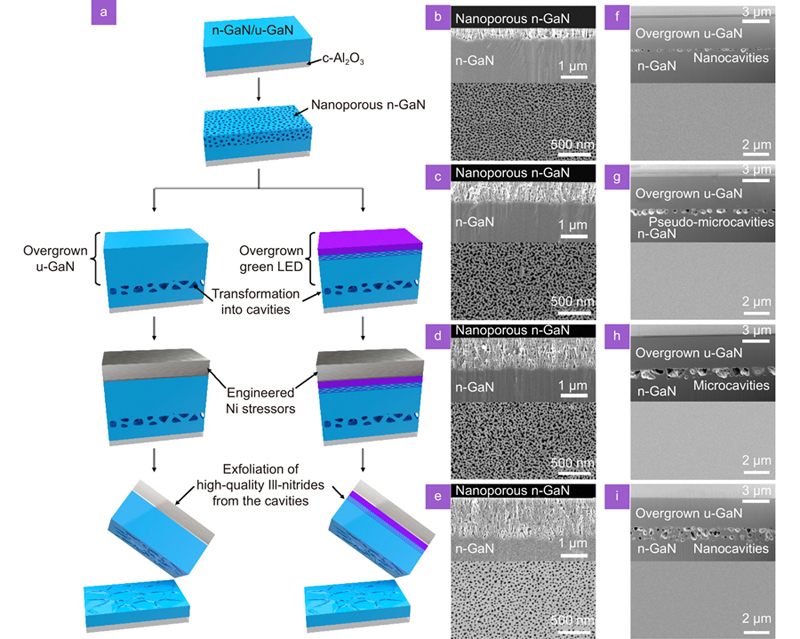
Herein, we propose a microcavity-assisted crack propagation method for the effective separation of tightly bonded III-nitride alloys. Figure 1(a) shows a representative schematic illustration of the exfoliation of III-nitride-based materials. Nanoporous structures originally having nanosized void spaces were formed by using EC etching of n-type GaN (n-GaN) layers. Afterward, single-crystalline III-nitride alloys, such as undoped GaN (u-GaN) and green LED structures, were overgrown on lattice-matched nanoporous structures by using metal organic chemical vapor deposition (MOCVD). The epitaxial growth of the III-nitride layers on the nanopores formed various sizes of cavities between the overgrown layers and the templates according to the porosity, depth of the nanoporous layer, and growth duration due to the rearrangement of the structures. This reformation effectively reduced the primary large interfacial toughness of GaN and led to a weaker interface. However, it was still insufficient to separate the overgrown layers from the cavity interface by using polymer or adhesive tape. In this work, tensile-stressed Ni layers (i.e., Ni stressors) were applied to provide sufficient external energy, and crack propagation easily occurred at the cavity interface as the energy release rate through the Ni stressor reached the reduced interfacial toughness.

Figure 1.(a) A summary of the schematic illustration for the exfoliation of large-scale and high-quality III-nitride layers through microcavity-assisted crack propagation to achieve membrane-based applications such as surface-emitting vertical-type green LEDs (V-LEDs), as well as surface-absorbing vertical-type ultraviolet photodetectors (V-UV PDs). (b–e) Scanning electron microscope (SEM) images of cross-sectional and top views for the nanoporous n-GaN layers manufactured by various EC etching conditions: 15 V for 5 min (b), 10 min (c), and 15 min (d) by using heavily doped n-GaN, and 20 V for 15 min (e) by using lightly doped n-GaN. In order, each nanoporous n-GaN is designated as ‘Nanoporous 1’, ‘Nanoporous 2’, ‘Nanoporous 3’, and ‘Nanoporous 4’. The porosity and depth of the nanoporous structures can be varied through the input voltage, time, and doping concentration. (f–i) Focused ion beam (FIB)-SEM and SEM images of cross-sectional and top views for the overgrown u-GaN layers. The overgrown u-GaN layers on the nanoporous structures are named ‘Overgrown u-GaN 1’, ‘Overgrown u-GaN 2’, ‘Overgrown u-GaN 3’, and ‘Overgrown u-GaN 4’. After overgrowing the u-GaN layers, cavities were formed with different shapes and sizes according to the original nanoporous structures.
Experimental section
Preparation of n-GaN templates
We prepared 2-inch c-Al2O3 substrates after cleaning organic residues and native oxide with acetone and HF. Epitaxial growth was conducted by using metal organic chemical vapor deposition MOCVD. After loading the substrates in a reactor in the MOCVD, we started the growth with thermal treatment at 1170 °C in ambient H2 under 100 Torr (1 Torr=133.3 Pa) for 10 mins. Subsequently, trimethylgallium (TMG), ammonia (NH3), and SiH4 were used as sources of GaN and Si dopants. Based on the sources, the 2-μm-thick u-GaN layer was grown at 1050 °C after growing the low-temperature (LT) buffer layer at 540 °C. Finally, n-GaN templates were prepared to create nanoporous layers by growing 5-μm-thick n-GaN with two types of doping concentrations, ~5 × 1018 cm–3for lightly doped and ~8 × 1018 cm–3 for heavily doped.
EC etching for nanoporous structures
To inject a current for EC etching, an electrode was formed at one edge of a 2-inch n-GaN template using indium soldering (
Fig. S1(a)). The n-GaN template and a Pt wire acting as counter electrodes were connected to a positive and a negative electrode, respectively, while immersing in 0.3 M oxalic acid prepared in a beaker. We applied 15 V and 20 V for n-GaN templates with ~8 × 1018 cm–3 and ~5 × 1018 cm–3 doping concentrations, respectively, while maintaining 50 mA compliance. Furthermore, we used different process times, such as 5, 10, and 15 min for heavily doped n-GaN templates and 15 min for lightly doped n-GaN templates, to control the porosities and depths of the nanoporous structures (
Fig. S1(b)).
Overgrowth of u-GaN and green LED
The 2-inch nanoporous n-GaN templates were ready in the reactor in MOCVD to overgrow u-GaN and green LED structures. First, an ~3.4-µm-thick u-GaN layer was directly grown by using TMG and NH3 at 1050 °C for 1.5 hours without the LT buffer layer. Second, the whole structure of the green LED consisted of ~2.4-μm-thick n-GaN, a relaxation layer, three pairs of InGaN/GaN (2 nm/9 nm) multiquantum wells (MQWs), a p-InGaN hole reservoir layer, and a 100 nm-thick p-type-doped GaN (p-GaN)/2-nm-thick p-InGaN layer for ohmic contact. The InGaN layer was grown by using trimethylindium, and the composition of the In was controlled by varying the temperature. The p-GaN layer was grown at 970 °C by flowing bicyclopentadienylmagnesium. The total growth time for the green LED structures was 8 hours. Finally, the p-GaN was activated by using a rapid thermal annealing process at 650 °C in 200 sccm ambient oxygen for 10 min.
Electroplating for Ni layers
A Ni layer is a good candidate for use as a stressor because residual tensile stress can be tailored according to the deposition method and conditions, such as sputter deposition and electroplating19-22. The electroplating of the Ni layer was conducted after depositing 50-nm-thick Ti and Ni layers for an adhesive and a seed layer through e-beam evaporation, respectively. The samples were connected to a homemade jig and dipped into NiSO4-based solution at 55 °C after a deionized (DI) rinse. The sample and a Ni plate were connected to a negative electrode and a positive electrode, respectively. By keeping a 20 cm distance between the jig and the Ni plate, the electroplating process was performed under ~ 70 mA/cm2 at ~ 2.5 V. After depositing the target thickness, the residual solution was rinsed by DI and dried by N2 blowing.
Residual stress measurement of the Ni stressor
The residual tensile stress for a Ni layer was measured through an ω-2θ scan of X-ray diffraction (XRD) with changing ψ. First, an ω-2θ scan was performed from 30° to 110° to check the positions related to Ni (
Fig. S5(a)). The Ni layer deposited by the electroplating was polycrystalline, showing multiple orientations, such as (111), (200), (202), (311), and (222). Ni (311) was used to measure the residual stress due to the strong peak intensity. By narrowing the range of the ω-2θ scan near Ni (311), the peak positions were measured by varying ψ to obtain the results of d-spacing versus sin2ψ (
Fig. S5(b)). Based on the change in d-spacing according to the variation in ψ, the residual stress can be obtained from the following equation:
where
,
,
, and
indicate Young’s modulus and Poisson’s ratio of the measured material, Bragg’s angles at stress-free, and variations of Bragg’s angles according to
, respectively. All the constants in the calculation referred to our previous results.
Exfoliation of the overgrown u-GaN and green LED
Target layers, such as a u-GaN layer and green LED layers overgrown on nanoporous structures, can be peeled off by applying external energy through tensile-stressed Ni layers by matching the reduced interfacial toughness, known as the critical Griffith’s energy release rate. The Griffith’s critical energy release rate is closely related to the interfacial toughness of the materials, and the interfacial toughness is proportional to the surface energy and inversely proportional to the surface area. In this work, the high interfacial toughness of GaN can be decreased by reducing the surface area according to the density of the cavities. In addition, the interfacial toughness for the other interfaces, such as GaN/Ti and Ti/Ni, should be larger than the reduced interfacial toughness through the cavity. The calculated interfacial toughness was obtained from the following equation:
where v, H, σ, and E represent the Poisson ratio, film thickness, residual stress, and Young’s modulus, respectively23.
Vertical green LEDs
A green LED membrane was prepared by exfoliating green LED layers from the cavities by using a Ni stressor. The photoresist (PR, ECI 3027) was coated on the top of the membrane by using spin-coating at 3000 rpm for 30 s and cured at 110 °C for 1 min. Mesa patterns were formed by exposing the samples by using a maskless aligner (Heidelberg μPG 501) and subsequently processed using the developer (AZ 726MIF) for 40 s. Then, the mesa structures were formed through dry etching by using ICP-RIE. To passivate the sidewall, an ~100 nm-thick SiO2 layer was deposited on the whole membrane. Then, patterns for revealing the metal contact regions were formed by using ECI 3027 with the same processes above. RIE was performed to open the n-metal pad regions. To form the metal contacts, lift-off resist (LOR 3A) was coated by using spin-coating at 3000 rpm for 30 s and cured at 110 °C for 5 mins. Additionally, ECI 3027 was covered with spin-coating and curing, and the metal patterns were made by a mask-less aligner and developed by using the same conditions above. Ti/Au (30 nm/100 nm) was deposited through sputtering, and metallization was completed by removing the PR and LOR 3A with acetone and developer, respectively.
Vertical UV PDs
A u-GaN membrane was ready by exfoliating the u-GaN layer from the cavities. All the residual n-GaN layer was removed by using ICP-RIE. Then, mesa structures were formed by using the same processes, such as coating with ECI 3027, exposure, and developing in the V-LED fabrication. Then, 100 nm-thick SiO2 was deposited for passivation on the whole membrane. To reveal metal pads and metallization, all the fabrication processes were the same as those used for V-LED fabrication.
Characterization
We utilized FEI Helios and Zeiss Merlin for the TEM lamella, FIB-SEM and normal SEM images. The residual stress and other XRD measurements were examined using a Bruker D8 Eiger and Bruker D8 Ultra diffractometer with Cu Kα (λ = 1.5405 Å, 1 Å=0.1 nm) radiation. Moreover, all materials subjected to XRD were examined by using CrystalDiffract software. The PL measurements for GaN-based layers and green LEDs were conducted by using a 325 nm He-Cd laser and a 473 nm Cobolt laser, respectively, manufactured by Witec Apyron. The TEM images and EDX mapping were obtained by an FEI Titan Themis at 300 keV. L5000 LED characteristic system manufactured by McScience Inc. was used for measuring membrane-based V-LEDs. In the system, a Keithley 2400 was used as a source measurement unit, and a CDS 1100 from Labsphere was used as a spectrometer. In addition, the photoelectrical performance of the V-UV PDs was tested using a broadband 500 W mercury–xenon [Hg (Xe)] arc lamp (Newport, 66142). The emitted light passed through a monochromator (Oriel CornerstoneTM, CS260) equipped with a UV-based diffraction grating (Newport, 74060) before illuminating the samples. The intensity of light was controlled using neutral density filters and precalibrated using a Si-based PD (Newport, 818-UV). The I–V characteristics of the PDs were extracted using a four-terminal sensing semiconductor parameter analyzer (Agilent, 4156C).
Results and discussion
Various sizes of cavity formation according to the nanoporous n-GaN
The porosity and depth of the nanoporous structures can be controlled depending on the doping concentration of n-GaN, the applied voltage, and the time24-26. In the present experiment, the nanoporous n-GaN layers were subjected to 15 V for 5 min (‘Nanoporous 1’, Fig. 1(b)), 10 min (‘Nanoporous 2’, Fig. 1(c)), and 15 min (‘Nanoporous 3’, Fig. 1(d)) by using heavily doped n-GaN layers (~8 × 1018 cm–3) and 20 V for 15 min (‘Nanoporous 4’, Fig. 1(e)) by using a lightly doped n-GaN layer (~5 × 1018 cm–3). The resultant nanoporous structures showed corresponding porosities of ~33.4%, ~44.9%, ~44.9%, and ~22.1% and depths of ~400 nm, ~800 nm, ~1.1 μm, and ~1.4 μm, respectively. In this work, we defined the porosity as the surface ratio of the area of voids to the total area. We were then able to grow fully coalesced ~3.4 μm-thick u-GaN layers on the various nanoporous n-GaN layers, as shown in Fig. 1(f–i). All the samples for the nanoporous and overgrown u-GaN were manufactured using 2-inch n-GaN templates, while the 2-inch nanoporous templates and overgrown u-GaN wafers were cleaved into ~1 cm2 pieces for further analysis and exfoliation (
Fig. S1). We directly performed the high-temperature growth condition without low-temperature buffer growth (see Experimental section). The overgrown u-GaN layers on ‘Nanoporous 1’, ‘Nanoporous 2’, ‘Nanoporous 3’, and ‘Nanoporous 4’ are designated ‘Overgrown u-GaN 1’, ‘Overgrown u-GaN 2’, ‘Overgrown u-GaN 3’, and ‘Overgrown u-GaN 4’, respectively. We clearly observed that the original nanoporous structures were transformed into various sizes of cavities depending on the original nanoporous structures after high-temperature growth at 1050 °C, which is higher than the decomposition temperature of GaN (~900 °C)27. That is, the entire nanoporous structures tend to rearrange into near-spherical shapes (
Fig. S2) because of the decomposition and diffusion of atoms that gathered from the larger curvature area to the smaller curvature of the nanoporous structures, which can be explained by Rayleigh instabilities28, 29. To investigate the quality of the overgrown u-GaN layers, we performed various XRD measurements, such as ω-2θ scan, ω rocking curve for the (002) orientation, ϕ scan for the (102) orientation, and ω rocking curve for the (102) orientation. Based on the results of the XRD measurement, we confirmed that all the overgrown u-GaN layers showed a full-width at half-maximum (FWHM) of ~300 arcsec, which indicates relatively high-quality overgrown films for both ω rocking curves for the (002) and (102) orientations (
Fig. S3). In addition, the photoluminescence (PL) measurement using 325 nm He-Cd laser excitation for the samples showed strong GaN near-band edge emission peaks (~3.42 eV), excitons bounded to surface defects (3.35 eV), and carbon-related defects (~3 eV)30-32. Minor peaks related to structural defects (~2.24 eV) were observed (
Fig. S4)32.
Microcavity-assisted crack propagation by engineering tensile-stressed Ni layers
Figure 2(a) shows a representative schematic illustration of the exfoliation of the u-GaN layers. The main idea is that we achieved a smaller interfacial toughness by reducing the bonding areas of GaN through cavity formation. An energy release rate greater than the reduced interfacial toughness is then applied through a Ni stressor to initiate crack propagation (see Experimental section). The energy release rate can be controlled through the residual tensile stress and the thickness of the electroplated Ni layers, and the residual tensile stress used here was 149 MPa (
Fig. S5). Figure 2(b) shows a summary of the evaluation of the exfoliation process. We referred to 6.38 J/m2 for the original interfacial toughness of c-plane GaN and investigated the changes in the interfacial toughness according to the density of the cavities. In this work, we defined the density of cavities as the ratio of voids over the total area after exfoliation. We first evaluated the possibility of exfoliation by using ‘Overgrown u-GaN 3’ for its largest voids, i.e., weakest interfacial toughness, as investigated by focused ion beam-scanning electron microscopy (FIB-SEM) images (Fig. 1(f–i)). The black dots in Fig. 2(b) are experimental data obtained from the electroplated Ni with different deposition times. We noted that the overgrown u-GaN began to be exfoliated from 2 J/m2 and fully exfoliated at 2.4 J/m2 for the calculated energy release rate of the Ni stressor. Then, exfoliation can be easily performed by pulling the Ni stressor using a metal tweezer (
Supplementary video 1). The u-GaN membrane exfoliated from the cavities is shown in Fig. 2(c). In contrast, it was hard to peel off the rest of the samples even if the energy was more than 2.4 J/m2 was applied with a Ni stressor. In addition, although the separation was forcibly performed, it was found that the u-GaN layers were partially separated at the cavity, and in most cases, separation occurred between the Ti and Ni layers (
Fig. S6). The main factor for partial exfoliation, except ‘Overgrown u-GaN 3’, originates from the different weakest interfaces in the samples. In all the samples, there are three major interfaces for crack propagation: i) cavity interfaces, ii) Ti/u-GaN, and iii) Ti/Ni. In this work, we treated the interface of Ti and u-GaN with O2 plasma (50 W in 20 sccm for oxygen) to increase the bonding strength of the interface. However, the interface at Ti/Ni is formed only with deposition through e-beam evaporation. Thus, the maximum energy release rate is bound by the interface bonding strength of Ti/Ni. Although the interfacial toughness of Ti/Ni is slightly different depending on the conditions of surface status and types of deposition, the range of 2.45–3.91 J/m2 has been reported33. For a more detailed interpretation, the substrate side regions, which were fully or locally peeled off, were investigated through SEM images (
Fig. S7). We observed similar trends in the changes in the size and shape of voids according to the initial states of the nanoporous structures, and the overall density of the cavities was also found to be different. Several micron-sized islands and voids formed from the cavities were observed in the case of ‘Overgrown u-GaN 3’, and we estimated that the density of the cavities was ~62.2% through image processing of the SEM image. In contrast, the rest of the overgrown u-GaN samples showed that submicron-sized voids were formed, and the estimated density of the cavities was ~38.2% for ‘Overgrown u-GaN 1’, ~51.1% for ‘Overgrown u-GaN 2’, and ~41.4% for ‘Overgrown u-GaN 4’. Based on the estimated density of the cavities, we were able to redefine the effective interfacial toughness of GaN depending on the different cavities as 3.94 J/m2 for ‘Overgrown u-GaN 1’, 3.12 J/m2 for ‘Overgrown u-GaN 2’, 2.41 J/m2 for ‘Overgrown u-GaN 3’, 3.74 J/m2 for ‘Overgrown u-GaN 4’, respectively. Except for ‘Overgrown u-GaN 3’, the effective interfacial toughness of the rest of the samples is larger than that of the Ti/Ni interface. That is, we are able to classify the following regions: i) subcritical region below ~2 J/m2 where crack propagation does not occur at values below 2 J/m2; ii) critical region where crack propagation proceeds from the interfacial toughness of 2 J/m2 to below 2.45 J/m2; iii) overcritical region where crack propagation occurs irregularly at the interface between the cavity interface and Ti/Ni. After exfoliating the overgrown u-GaN layer, several microsized islands are observed on both the membrane side and the substrate side (Fig. 2(d) and 2(e)). In addition, we clearly observed the ~3.4 μm-thick u-GaN membrane with Ti/Ni stressor and ~200 nm-thick remaining n-GaN layer through cross-sectional FIB-SEM, and ~800 nm-thick microsized n-GaN islands remained on the substrate side. To investigate the quality of the u-GaN membrane, we performed various XRD measurements (Fig. 2(f–i)). The XRD peak positions of GaN (002) and Ni (111) were measured at 34.5° and 44.7° in the u-GaN membrane, respectively, and sixfold symmetry appeared in the (102) orientation. Furthermore, the FWHM values for the ω rocking curve for the (002) and (102) orientations were 356.9 arcsec and 364.9 arcsec, respectively. Based on the results of the ω rocking curve, we confirmed that the quality of the u-GaN membrane is comparable to that before exfoliation. Furthermore, we measured PL before and after exfoliation (
Fig. S8). Based on the reference PL for ‘Overgrown u-GaN 3’ (
Fig. S8(a)), we clearly observed that there were no additional peaks related to u-GaN because n-GaN layers were exposed at the top surface immediately after exfoliation (
Fig. S8(b) and
S8(c)). However, the subpeaks related to u-GaN reappeared when the n-GaN top layer was removed by ICP-RIE etching (
Fig. S8(d)).
Figure 2.(a) A representative schematic illustration of microcavity-assisted crack propagation. (b) The values of the interfacial toughness of GaN depending on the density of the cavities (blue-colored line) and the applied interfacial toughness through the Ni stressors (black-colored line). The maximum value of the interfacial toughness is 6.38 J/m2 with reference to GaN (002). The blue- and black-colored spheres are the experimental data points obtained from the estimated cavity densities and Ni stressors, respectively. (c) A digital camera image of a u-GaN membrane acquired from ‘Overgrown u-GaN 3’ after successful exfoliation with the well-engineered Ni stressor. The inset shows the substrate side after exfoliation. (d–e) Representative schematic illustrations for the u-GaN membrane side and the substrate side and the related SEM and FIB-SEM images for the top, bird’s eye, and cross-sectional views, respectively. The microsized islands were observed on the surface of the membrane and the substrate after exfoliation. (f–i) Results of the various XRD measurements to check the quality of the u-GaN membrane after exfoliation: ω-2θ scan (f), ω rocking curve for (002) orientations (g), ϕ scan for (102) orientations (h), and ω rocking curve for (102) orientations (i).
Exfoliation of green LED structures
In addition to the homogeneous u-GaN membranes, we were able to apply the cavity-assisted exfoliation process in producing heterogeneous III-nitride membranes for further optoelectronic applications. In this work, we grew green LED structures based on the previous nanoporous structures except ‘Nanoporous 4’, which has a low porosity (
Fig. S9 and Fig. 3(a)). Importantly, the formation of cavities for the overgrown green LED structures was totally different from that for the overgrown u-GaN layer. Although green LED structures were properly grown on ‘Nanoporous 1’ and ‘Nanoporous 2’, the green LED structures on ‘Nanoporous 3’ were unmerged even under the same growth conditions. In addition, we observed that the cavities formed in the overgrown green LED were much wider than those of the overgrown u-GaN even when using the same nanoporous structures. We speculate that this wider cavity formation and the failure of overgrowth in ‘Nanoporous 3’ were attributed to a much longer exposure time (~8 hours) at higher temperatures (> 900 °C), leading to a more severe structural rearrangement of nanoporous GaN layers. We representatively investigated the green LED structures overgrown on ‘Nanoporous 2’ using SEM, FIB-SEM, scanning transmission electron microscopy (STEM), and STEM-energy dispersive X-ray (EDX) (Fig. 3(a)). We clearly identified smooth surface and micron-sized cavities through SEM and FIB-SEM images. The green LED has the following structure: n-GaN/n-InGaN (relaxation layer)/MQWs/p-InGaN (hole reservoir layer)/p-GaN/p-InGaN (Ohmic contact layer). Based on the overgrown green LED on ‘Nanoporous 1’ and ‘Nanoporous 2’, we performed exfoliation of the green LED layers from the cavities by using the Ni stressor with the same energy release rate as the ‘Overgrown u-GaN 3’ case (~2.4 J/m2). Although the green LED structures overgrown on ‘Nanoporous 1’ were partially peeled off, we succeeded in exfoliating the green LED structures overgrown on ‘Nanoporous 2’ (Fig. 3(b)). The overall exfoliation process of the green LED is described in
Supplementary video 2. After exfoliation, PL measurements were conducted for the overgrown green LED, the green LED membrane side, and the substrate side (Fig. 3(c)). The green LED membrane showed a PL peak wavelength of ~533 nm, while the substrate side showed only a GaN-related peak at ~362 nm and an oxygen vacancy-related yellow emission peak at ~550 nm. Importantly, net-like microsized islands are formed on the surface of the green LED membrane and substrate side, unlike in the case of u-GaN (Fig. 3(d) and 3(e)). The differences were clearly revealed in the optical microscope images (
Fig. S10(b)). Obvious net-like islands were found on both the membrane and substrate side for the case of green LED, unlike that of u-GaN (dot-like islands). Furthermore, we investigated the density of the cavities using the same estimation described above and obtained a value of ~63%, which is similar to the case of ‘Overgrown u-GaN 3’ (
Fig. S10(a)). From the exfoliation results of the u-GaN and green LED layers, we have been convinced that the primary strong interfacial toughness can be controlled by using cavity formation according to porosity, depth, and even growth conditions, and the target layers can be easily peeled off from the cavity by matching the energy release rate of the Ni stressor to the reduced interfacial toughness mentioned above.
Figure 3.(a) SEM images of the top and cross-sectional views for an overgrown green LED on ‘Nanoporous 2’. The blue-colored dash indicates the detailed top-most areas of the green LED through a high-angle annular dark-field scanning transmission electron microscope (STEM) image and the related STEM-energy dispersive X-ray analysis mapping. (b) A digital camera image of a green LED membrane exfoliated from cavities with a well-engineered Ni stressor. The inset shows the substrate side after exfoliation. (c) Results of photoluminescence of the green LED before and after exfoliation. The 473 nm Cobolt laser was used for the as-grown green LED and the green LED membrane due to the peak wavelength of the green LED (~533 nm), and the He-Cd 325 nm laser was employed for the substrate side. (d-e) Representative schematic illustrations for the green LED membrane side and the substrate side and the related SEM and FIB-SEM images for the top, bird’s eye, and cross-sectional views, respectively. Wider microsized islands were observed on the surfaces of the membrane and the substrate compared to the u-GaN membrane.
Device applications based on III-nitride membranes
Based on III-nitride membranes, we proceed to demonstrate surface-emitting vertical-type green LEDs (V-LEDs) without an additional current spreading layer (CSL), as well as surface-absorbing vertical-type ultraviolet photodetectors (V-UV PDs). The electroplated Ni layer used as a stressor for exfoliation can also be used as a metal substrate after removing the original insulating substrate. The overall fabrication process for both devices is shown in
Fig. S11 for the V-LEDs and
Fig. S12 for the V-UV PDs. We investigated the V-LEDs through current density-voltage characteristics, electroluminescence (EL) spectra, and EL images (Fig. 4(a–c)). The peak wavelength of the V-LED was ~ 525 nm. In addition, the turn-on voltage was 2.8 V, and the current spread out well even without additional CSLs, such as ITO and Ni/Au, because the electroplated Ni layer can act as a bottom electrode, unlike conventional lateral-bottom-contact LEDs based on insulating substrates. In addition to the V-LEDs, we also fabricated V-UV PDs by using the u-GaN membrane and investigated the overall properties, such as current voltages, responsivity, linear dynamic range (LDR), and time response (Fig. 4(d-i)). We selected 360 nm as the primary wavelength to investigate the current-voltage characteristics of the V-UV PDs, such as dark current (Idark) and photocurrent (Iphoto), from 0 V to −5 V. The V-UV PDs showed clear Ohmic contact characteristics and a low Idark of 4.82 × 10⁻¹⁰ A at −5 V, which correspond to a current density of 5.55 × 10⁻⁷ A/cm2 at −5 V. Under light illumination of 360 nm, the value of Iphoto was 2.98 × 10⁻⁶ A at −5 V, and the ratio of Iphoto and Idark was 1.15 × 10³ at −5 V. The responsivity of the V-UV PDs was obtained by the ratio of Iphoto and Idark with varying wavelengths (Fig. 4(e)). The V-UV PDs showed high selectivity of the wavelength at 360 nm, and the peak responsivity was 8.78 A/W at -5 V under 360 nm illumination. In addition, the LDR reached 73.68 dB from the current density by varying light intensities from 1.39 × 10⁻³ to 6.71 mW/cm2 under 360 nm illumination at −5 V (Fig. 4(f)). Moreover, we also measured the time response of the V-UV PDs based on a modulated frequency of 1 kHz, and the rise time and fall time were 145 μs and 205 μs, respectively.
Figure 4.Device applications using green LEDs and u-GaN membranes. (a–b) Current density-voltage and electroluminescence (EL) spectral characteristics of the V-LEDs. The peak wavelength of the V-LEDs was ~525 nm. (c) Optical microscope EL images of the green V-LEDs according to input voltages. (d) Current–voltage characteristics of the V-UV PDs under illumination at 360 nm (0.53 mW/cm2). (e) Responsivity of the V-UV PDs at –5 V according to wavelengths from 300 nm to 440 nm. The peak responsivity was 8.78 A/W at 360 nm, and the responsivity spectrum showed a high selectivity of the wavelength over 350−370 nm. (f) Measured values of the current density depending on the illuminated light intensity from 1.39 × 10⁻³ to 6.71 mW/cm2 at –5 V. (g) Time response characteristics measured by using a 375 nm laser diode at –5 V. The UV laser pulses were 1 kHz. (h-i) The zoom-in time response curve and its biexponential fitting curves to obtain the rise time and decay time. The rise and decay times are 145 and 205 μs, respectively.
Conclusion
In conclusion, we have demonstrated large-scale and high-quality III-nitride membranes, such as green LED membranes and u-GaN membranes, through the microcavity-assisted crack propagation method. The original large interfacial toughness of GaN can be effectively reduced by shrinking the effective surface areas through microsized cavities formed between the overgrown layers and the n-GaN templates, and the overgrown layers can be peeled off at the cavity interfaces through a well-engineered Ni stressor. The III-nitride membranes showed high structural and optical quality, and operational optoelectronic membranes were also demonstrated, such as CSL-free V-LEDs and V-UV PDs. This microcavity-assisted crack propagation technique can be applied to exfoliate other tightly bonded semiconductors, which can open many pathways for promising device improvement and applications such as vertical, flexible, and thermal-manageable devices and heterogeneous integration based on large-scale and high-quality semiconductor membranes.
Acknowledgements
The work was supported by King Abdullah University of Science and Technology (KAUST) baseline funding BAS/1/1614-01-01 and King Abdulaziz City for Science and Technology (Grant No. KACST TIC R2-FP-008). This work was also supported by Korea Photonics Technology Institute (Project No. 193300029). The authors acknowledge access to the KAUST Nanofabrication Core Lab for device fabrication and Imaging and Characterization Core Lab for optical and electron microscopy measurements.
B. S. Ooi supervised the work. J. H. Min designed and conducted experiments and analysis and prepared the manuscript. K. J. Lee designed experiments and fabricated nanoporous structures. T. H. Chung grew III-nitride structures. J. W. Min and K. H. Li prepared FIB and TEM samples. C. H. Kang measured the devices. Y. Yuan measured XRD. All authors discussed the results and implications, and commented on the manuscript at all stages.
The authors declare no competing financial interests.
Supplementary information for this paper is available at https://doi.org/10.29026/oes.2022.220016