
Tingting Zeng, Meiping Zhu, Yingjie Chai, Jingping Li, Jianda Shao. Dichroic laser mirrors with mixture layers and sandwich-like-structure interfaces[J]. Photonics Research, 2021, 9(2): 229
- Photonics Research
- Vol. 9, Issue 2, 229 (2021)
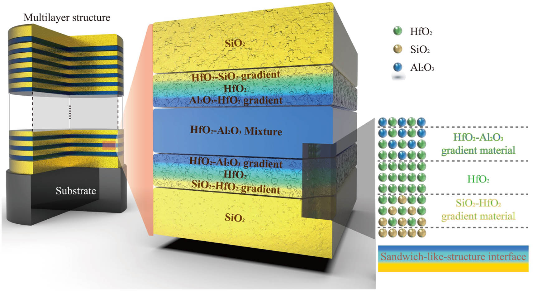
Fig. 1. Schematic diagram of the proposed MDLM design.
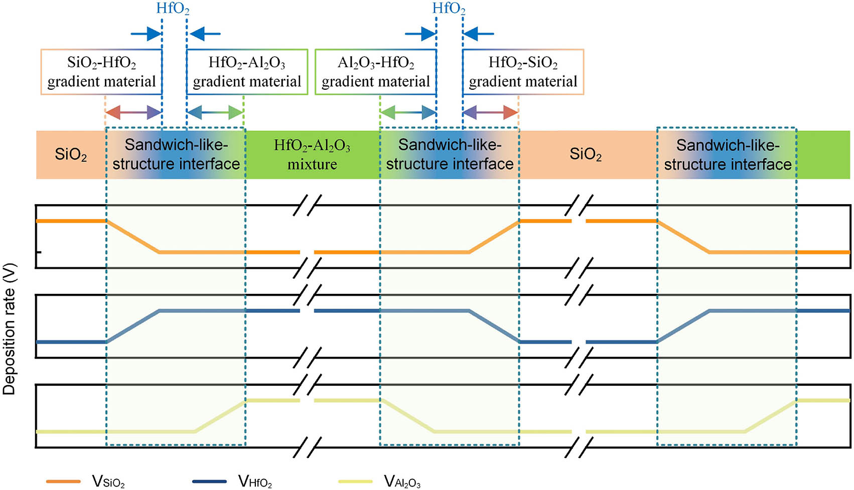
Fig. 2. Schematic diagram of the deposition process of MDLM coating.
Fig. 3. Microstructure and optical property of the pure monolayer, nanolaminate, and mixture coatings. (a) XRD spectra, (b) transmittance, and (c) optical bandgap versus n HfO 2 Al 2 O 3 HfO 2 − Al 2 O 3 Δ Power HfO 2 − Al 2 O 3
Fig. 4. Dispersion curves of refractive indices of HfO 2 Al 2 O 3 HfO 2 − Al 2 O 3
Fig. 5. Elemental percentage profiles from the high-n n
Fig. 6. Microstructure and optical property of the TDLM and MDLM coatings. (a) XRD spectra. (b) Transmittance (left: incident angle at 0°; middle: incident angle at 45°, p s
Fig. 7. Damage morphology imaged by SEM and the depth profile of the marked area measured by FIB. (a)–(d) Damaged sites and (e)–(h) schematic diagram of the damage morphologies after irradiation of an s s
Fig. 8. Damage morphology imaged by SEM and the depth profile of the marked area measured by FIB. (a) and (b) Full field-of-view of the damaged area. (c)–(i) Typical damaged sites marked with asterisks. (j)–(m) Schematic diagram of the damage morphologies after irradiation of a p
Fig. 9. EDS characterized chemical composition of the damaged site of the TDLM coating and MDLM coating induced by 1064 nm p
Fig. 10. Simulated laser-induced temperature rises in TDLM and MDLM coatings.
| |||||||||||||||||||||||||||
Table 1. Design Information and Extracted Thickness of the Nanolaminate Coatingsa
|
Table 2. Extracted Defect Parameters

Set citation alerts for the article
Please enter your email address
© Copyright 2018-2021 | Chinese Laser Press. All Rights Reserved 沪ICP备15018463号-20