• Journal of Semiconductors
  • Vol. 43, Issue 12, 122101 (2022)
Tieshi Wei1、2, Xuefei Li1、*, Zhiyun Li3, Wenxian Yang1, Yuanyuan Wu1, Zhiwei Xing1, and Shulong Lu1、**
Author Affiliations
  • 1Key Laboratory of Nanodevices and Applications, Suzhou Institute of Nano-Tech and Nano-Bionics, Chinese Academy of Sciences, Suzhou 215123, China
  • 2Nano Science and Technology Institute, University of Science and Technology of China, Suzhou 215123, China
  • 3Vacuum Interconnected Nanotech Workstation (NANO-X), Suzhou Institute of Nano-Tech and Nano-Bionics, Chinese Academy of Sciences, Suzhou 215123, China
  • show less
    DOI: 10.1088/1674-4926/43/12/122101 Cite this Article
    Tieshi Wei, Xuefei Li, Zhiyun Li, Wenxian Yang, Yuanyuan Wu, Zhiwei Xing, Shulong Lu. Interfacial dynamics of GaP/Si(100) heterostructure grown by molecular beam epitaxy[J]. Journal of Semiconductors, 2022, 43(12): 122101 Copy Citation Text show less
    (Color online) Schematic illustration GaP/Si(100) heterostructure samples used in this work. (a) P-riched sample and (b) Ga-riched sample.
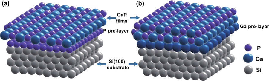
    Fig. 1. (Color online) Schematic illustration GaP/Si(100) heterostructure samples used in this work. (a) P-riched sample and (b) Ga-riched sample.
    (Color online) (a) Triaxial HRXRDω–2θ curves measured in the vicinity of Si (004) reflection for samples grown on Si substrates. AFM image (1 × 1μm2) of GaP grown on the Si (100) substrate surface with (b) P-riched and (c) Ga-riched.
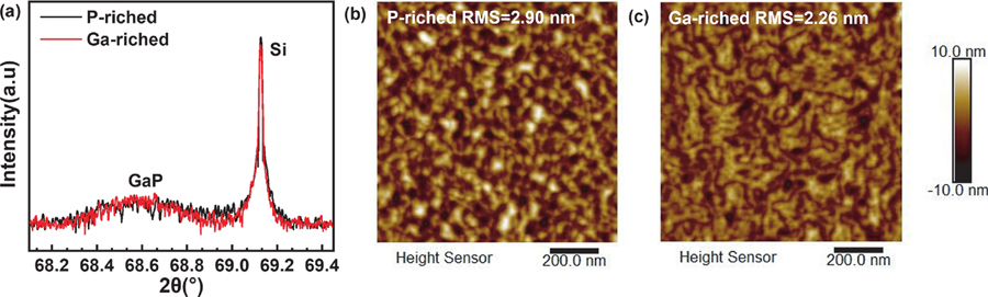
    Fig. 2. (Color online) (a) Triaxial HRXRDω–2θ curves measured in the vicinity of Si (004) reflection for samples grown on Si substrates. AFM image (1 × 1μm2) of GaP grown on the Si (100) substrate surface with (b) P-riched and (c) Ga-riched.
    (Color online) Dependence of (a, b) P 2p and (c, d) Ga 3d core level spectra on sputtering depth as a function of binding energy.
    Fig. 3. (Color online) Dependence of (a, b) P 2p and (c, d) Ga 3d core level spectra on sputtering depth as a function of binding energy.
    (Color online) High-resolution spectra measured on non-sputtered (0 nm) GaP/Si (100) samples with Si substrate surface (a) Ga-riched and (b) P-riched. Fits contain Ga0 (blue), Ga–P (red) and Ga–O (green) components. It can be seen that there are a small amount of Ga–O bonds and Ga–Ga metal bonds on the GaP/Si surface.
    Fig. 4. (Color online) High-resolution spectra measured on non-sputtered (0 nm) GaP/Si (100) samples with Si substrate surface (a) Ga-riched and (b) P-riched. Fits contain Ga0 (blue), Ga–P (red) and Ga–O (green) components. It can be seen that there are a small amount of Ga–O bonds and Ga–Ga metal bonds on the GaP/Si surface.
    (Color online) High-resolution spectra sputtered 26, 30 and 33 nm GaP/Si (100) samples with substrate (a–c) Ga-riched and (d–f) P-riched. Fits contain Ga0 (blue) and Ga–P (red) components.
    Fig. 5. (Color online) High-resolution spectra sputtered 26, 30 and 33 nm GaP/Si (100) samples with substrate (a–c) Ga-riched and (d–f) P-riched. Fits contain Ga0 (blue) and Ga–P (red) components.
    (Color online) Variation of Ga 3d component Ga0 metal bond, Ga-P bond (a, b) binding energy, and (c, d) corresponding bonding bond concentration with sputtering depths when the surface of Si substrate surface is P-riched and Ga-riched atoms. (The blue solid line refers to the GaP/Si heterointerface, and the blue dotted line refers to the position of XPS measured by Ar ion sputtering.)
    Fig. 6. (Color online) Variation of Ga 3d component Ga0 metal bond, Ga-P bond (a, b) binding energy, and (c, d) corresponding bonding bond concentration with sputtering depths when the surface of Si substrate surface is P-riched and Ga-riched atoms. (The blue solid line refers to the GaP/Si heterointerface, and the blue dotted line refers to the position of XPS measured by Ar ion sputtering.)
    High-resolution cross-sectional TEM image of the interface of GaP epitaxial layer grown on Si (100) substrate surface with (a, b) P-riched or (c, d) Ga-riched.
    Fig. 7. High-resolution cross-sectional TEM image of the interface of GaP epitaxial layer grown on Si (100) substrate surface with (a, b) P-riched or (c, d) Ga-riched.
    Tieshi Wei, Xuefei Li, Zhiyun Li, Wenxian Yang, Yuanyuan Wu, Zhiwei Xing, Shulong Lu. Interfacial dynamics of GaP/Si(100) heterostructure grown by molecular beam epitaxy[J]. Journal of Semiconductors, 2022, 43(12): 122101
    Download Citation