1Key Laboratory of Nanodevices and Applications, Suzhou Institute of Nano-Tech and Nano-Bionics, Chinese Academy of Sciences, Suzhou 215123, China
2Nano Science and Technology Institute, University of Science and Technology of China, Suzhou 215123, China
3Vacuum Interconnected Nanotech Workstation (NANO-X), Suzhou Institute of Nano-Tech and Nano-Bionics, Chinese Academy of Sciences, Suzhou 215123, China
The atomic structure and surface chemistry of GaP/Si(100) heterostructure with different pre-layers grown by molecular beam epitaxy are studied. It is found that GaP epilayer with Ga-riched pre-layers on Si(100) substrate has regular surface morphology and stoichiometric abrupt heterointerfaces from atomic force microscopes (AFMs) and spherical aberration-corrected transmission electron microscopes (ACTEMs). The interfacial dynamics of GaP/Si(100) heterostructure is investigated by X-ray photoelectron spectroscopy (XPS) equipped with an Ar gas cluster ion beam, indicating that Ga pre-layers can lower the interface formation energy and the bond that is formed is more stable. These results suggest that Ga-riched pre-layers are more conducive to the GaP nucleation as well as the epitaxial growth of GaP material on Si(100) substrate.The atomic structure and surface chemistry of GaP/Si(100) heterostructure with different pre-layers grown by molecular beam epitaxy are studied. It is found that GaP epilayer with Ga-riched pre-layers on Si(100) substrate has regular surface morphology and stoichiometric abrupt heterointerfaces from atomic force microscopes (AFMs) and spherical aberration-corrected transmission electron microscopes (ACTEMs). The interfacial dynamics of GaP/Si(100) heterostructure is investigated by X-ray photoelectron spectroscopy (XPS) equipped with an Ar gas cluster ion beam, indicating that Ga pre-layers can lower the interface formation energy and the bond that is formed is more stable. These results suggest that Ga-riched pre-layers are more conducive to the GaP nucleation as well as the epitaxial growth of GaP material on Si(100) substrate.
Introduction
Monolithically integration of III–V semiconductor on silicon (Si) substrate has shown high potential on optoelectronic devices, such as photodetectors, multijunction solar cells, laser diodes, and so on[1-5]. Though there are many obvious advantages of Si-based electronics, such as the cost-efficient, highly integrated, mature large-area fabrication process, and so on.[6,7], it is challenging to grow high-quality III–V materials on Si(100) because massive defects would arise on account of large lattice mismatch. Furthermore, antiphase domains (APDs), stacking faults (SFs), and micro-twins (MTs) are common defects for epitaxial growth due to polarity mismatch[8-10]. The lattice mismatch is only 0.37% between gallium phosphide (GaP) and Si with lattice constants of 5.45 and 5.43 Å, respectively[11,12]. In this regard, GaP is a suitable candidate as virtual template for further III–V/Si monolithically integration. Meanwhile, molecular beam epitaxy (MBE) can accurately control the composition and form an abrupt heterointerface, which makes it an important epilayer growth technique for semiconductor materials.
Little work has been reported to obtain a good GaP epilayer with low defect densities on Si by MBE. One of the key restrictive factors is the lack of well-defined and abrupt GaP/Si(100) heterointerface preparation. Lucciet al.[13] showed that a layer gallium (Ga) atomic at the interface is beneficial to GaP/Si(100) by calculation using density functional theory. Hoolet al.[14] implemented a two-step growth design to improve the quality of relaxed GaP on pseudomorphic GaP/Si templates by reducing the threading dislocation density (TDD) using MBE technology, but they only studied the relaxation state of GaP epitaxy on GaP/Si template without exploring the dynamical process at the heterogeneous interface. Recently, Romanyuket al.[15] reported the GaP grown on the P-riched Si substrate by using metal oxide vapor phase epitaxy (MOVPE), and the buried GaP/Si(100) heterointerfaces were analyzed by X-ray photoelectron spectroscopy (XPS). However, how the interface is formed at the atomic scale is still unclear. In the process of III–V nucleation under non-equilibrium conditions, the surface chemistry of Si substrate will determine the electronic structure of the whole interface, and it is very important for defects reduction to the subsequent epitaxial layer. In order to reduce the APDs density, it is necessary to better understand the basic physical and chemical processes at GaP/Si(100) heterointerface in the initial stage.
In this paper, we report on the growth of GaP/Si(100) heterostructures with different atoms (Ga or P) enriched at the initial stage by MBE. The heterointerface dynamics of GaP/Si(100) heterostructure are investigated by XPS method using Ar gas cluster ion beam (GCIB). In addition, the effect of pre-atom on the morphology and structural properties of GaP layer is also studied by atomic force microscopy (AFM), high-resolution X-ray diffraction (HRXRD), and spherical aberration-corrected transmission electron microscope (ACTEM).
Experiments
All GaP samples are grown on nominally (100)-oriented Si substrates in Veeco GEN20A MBE system with standard effusion cells for gallium and cracker cell for phosphorus. Before deposition, the Si(100) substrates are chemically cleaned using the standard Radio Corporation of America (RCA) clean method[3,16], the cleaned substrates are immediately subjected to pre-preparation module for 1 h at 350 °C, and then transferred to the growth chamber, followed by desorption at 1000 °C for 10 min to remove the remaining silicon oxide. Ga pre-layers (noted as Ga-riched) and P pre-layers (noted as P-riched) are sputtered on the Si(100) substrates at 440 °C, as a pre-nucleation prior to the growth of GaP epitaxial layers. Afterwards, GaP are grown by using migration enhanced epitaxy (MEE) under the same growing conditions. The deposition loop, which consisted of a sequence of 5 s Ga deposition, 1 s pause with closed Ga and P source, 8 s exposure under P flux, and 5 s pause, is repeated for 216 cycles. The P to Ga flux ratio is set at 8 : 1. The nominal thickness of GaP is 30 nm, which is well below the GaP/Si critical thickness[12,17].
The surface morphology of the GaP/Si is evaluated by AFM measurement (Bruker Dimension ICON), and the structural property is studied by high-resolution XRD measurement (Bruker Dimension D8 Discover). The binding bond of GaP samples, especially at the heterointerface between Si(100) substrate and GaP is analyzed by XPS technology using monochromatized AlKα radiation (1486.6 eV) in Thermo Scientific ESCALAB Xi+ photoelectron spectrometer equipped with GCIB. The ion beam current was 10μA for cluster ions with an energy of 4 keV and 1000 Ar atoms in the cluster. The diameter of the cluster ion beams was 0.3 mm and the sputtered area was 1.5 × 1.5 mm2. The cross-section of GaP/Si(100) heterostructures was characterized by spherical aberration-corrected transmission electron microscope (FEI Themis Z).
Results and discussion
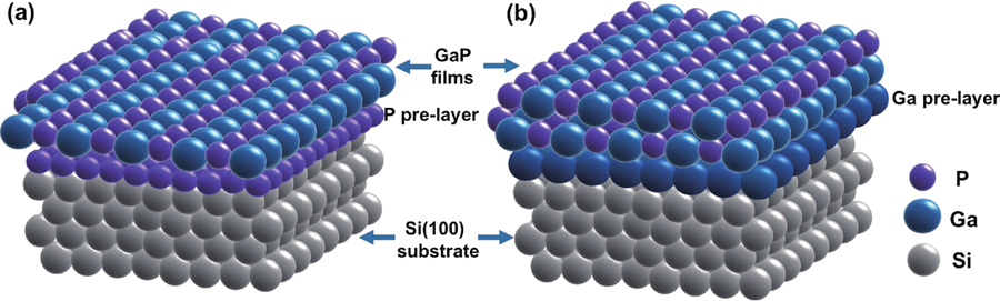
Fig. 1 presents atomic structure of the GaP samples with different Ga or P pre-layers on Si(100) substrate.
Figure 1.(Color online) Schematic illustration GaP/Si(100) heterostructure samples used in this work. (a) P-riched sample and (b) Ga-riched sample.
Triaxial HRXRDω–2θ curves are measured in the vicinity of Si(004) reflection for P-riched and Ga-riched samples. As shown inFig. 2(a), GaP and Si diffraction peaks can be observed. According to HRXRD, the lattice constants of GaP (5.467 Å) can be derived by using Bragg’s law and the calculation formula of interplanar crystal spacing of face-centered cubic structure[18]:
Figure 3.(Color online) Dependence of (a, b) P 2p and (c, d) Ga 3d core level spectra on sputtering depth as a function of binding energy.
whered is face spacing,θ is the Bragg angle in the vicinity of GaP(004),
(1.5406 Å) is wavelength of Cu Kα.Figs. 2(b) and2(c) show the surface mophorlogy of P-riched and Ga-riched pre-layers samples. The root mean square (RMS) roughness is 2.90 and 2.26 nm for P-riched and Ga-riched samples, respectively. The roughness of Ga-riched sample is smaller than that of P-riched sample. As we know, P atoms exposure to the Si (100) substrate surface results in atomic displacement of Si atoms by P atoms, and then, single-height islands are formed. The incorporated P atoms combine with Si atoms to form Si–P, so the Si(100) surface becomes roughened[19-21]. Furthermore, the P pre-layers covered Si(100) surface is expected to exhibit reduced chemical reactivity and an increased surface energy due to the filled P dangling bonds. While Ga pre-layers are known to adsorb to the Si(100) substrate surface, passivating the highly energetic Si dangling bonds and lowering the surface energy[21]. It is reasonable to conclude that the Ga-riched Si(100) substrate is more conducive to the arrangement of Ga atoms at the GaP/Si heterostructure.
Fig. 3 shows the dependence of P 2p and Ga 3d core level spectra on sputtering depth as a function of binding energy. The binding energy of 2P3/2 and 2P1/2 remains unchanged with sputter depth, as shown inFigs. 3(a) and3(b), which can be ascribed to the P-Ga bonding[22]. The binding energy of Ga 3d shift slightly in GaP/Si(100) material at different sputter depth, as expected. The Ga 3d core level peak maxima of P-riched sample have shifted towards lower binding energy by –0.56 eV with respect to the corresponding as-received spectra. However, the shift is –0.51 eV for Ga-riched sample, as shown inFigs. 3(c) and3(d). The shift is similar for both Ga 3d and P 2p core level peaks, which is induced by surface band bending, and oxide and carbon contaminations have been reduced significantly, up to the defects that are introduced by sputtering[15,22-24]. In addition, it can be seen that there are raised signals (labeled in the red dotted line area in theFigs. 3(c) and3(d)) that appear at the binding energy of Ga 3d peak, which represents the Ga0 component. The position of Ga0 component shifted 0.39 and 0.41 eV compared to that of Ga 3d component in Ga-riched and P-riched samples, respectively. This binding energy position shift corresponds to the Ga–Ga binding bond in the Ga metallic phase. With the increase of sputtering depth, the composition of Ga0 becomes higher at GaP/Si heterointerface in the Ga-riched sample, which is more obvious than that of P-riched sample. During the sputtering, phosphorus is first removed from the GaP compound on the surface or in bulk. Therefore, metallic nanoparticles or droplets are formed[25]. The surface energy band bending induced by oxide and carbon contaminations can lead to surface clean problems[15]. More importantly, the defects produced in the sputtering process are the main reason for the band bending.
Figure 5.(Color online) High-resolution spectra sputtered 26, 30 and 33 nm GaP/Si (100) samples with substrate (a–c) Ga-riched and (d–f) P-riched. Fits contain Ga0 (blue) and Ga–P (red) components.
Fig. 4 shows the Ga 3d core level spectra and fitting peaks on the surface of P-riched and Ga-riched GaP samples, respectively. The as-received spectra of the P-riched and Ga-riched samples contain bulk components (Ga0 and Ga–P) and oxide component (Ga–O). Both samples contain a large number of Ga-P bonds, as well as a small amount of Ga0 metal bonds and Ga–O oxide bonds. The binding energy of Ga–P, Ga0, and Ga–O (non-sputtered) are at 18.45, 17.75, and 19.47 eV, symbolished by blue, green and red color, respectively.
Figure 7.High-resolution cross-sectional TEM image of the interface of GaP epitaxial layer grown on Si (100) substrate surface with (a, b) P-riched or (c, d) Ga-riched.
Fig. 5 shows the experimental spectra and fitting results at the sputtered depth of 26, 30 and 33 nm of GaP/Si (100) samples. Considering the growth characteristics of MBE, only Ga–P binding bond and metal-binding bond are applied to decompose the experimental curve. It can be seen that the proportion of Ga–P binding bond is more than Ga0 metal-binding bond in the P-riched sample. As shown inFigs. 5(d)–5(f), the peak positions of Ga–P binding bond and Ga0 metal bond move towards low binding energy. At the minimum of Ga–P and Ga0 component binding bond energy (i.e., at the 30 nm), their binding energies are 18.24 and 17.75 eV in the Ga-riched sample, respectively. This shows that the state of Ga–P binding bond and Ga0 binding bond are increasingly stable in the GaP materials, and Ga–P binding bond is the most abundant in the GaP material[23]. However, the Ga0 metal bond component is comparable with Ga–P binding bond component at the sputter depth of 30 nm in the Ga-riched GaP sample. The Ga0 metal-binding bond component is less than the Ga–P binding bond component in the P-riched GaP sample. According to this description, the proportion of Ga0 metal bond is relatively high at 30 nm. This happens because it is close to the surface of Si(100) substrate and contains more Ga0 metal-binding bond in Ga-riched sample[22].
Image Infomation Is Not Enable
To further study the interfacial dynamics of GaP material on Si (100) substrate, the variation of binding energy of Ga 3d component in Ga-riched and P-riched GaP samples with sputtering depths is shown inFigs. 6(a) and6(b). The binding energy of Ga0 metal-binding bond and Ga–P binding bond at the interface decreases gradually in the P-riched GaP sample, as shown inFig. 6(a). However, metallic phase binding energy decreased with sputter depth until at 30 nm, and then slowly rose as the sputter process continues. It should be noted that the binding energy of Ga–P binding bond component at the GaP/Si interface decreases and the contents of Ga atoms in the compound phase or Ga metal elemental phase at the interface decreases[25].Figs. 6(c) and6(d) show the depth profiles of sputtered GaP/Si (100), indicating that the concentration of Ga 3d binding bond for both Ga-riched and P-riched samples changes with sputtering depths. Similar to that observed on sputtered GaP material, a Ga metallic phase (Ga0 cluster/droplets) is formed at the GaP/Si(100) heterointerface, while the Ga/P stoichiometry ratio remains unchanged (excluding the Ga0 contributions)[15]. In the Ga-riched GaP/Si(100) sample, the Ga0 concentration increases from the surface to about ~30 nm and then, decreases after ~30 nm. While the concentration of Ga–P binding bond show the opposite trend. In addition, when the concentration of Ga0 increases to the sputtering depth of ~33 nm, its concentration gradually decreases. This shows that with the increase of sputtering depths, a layer of Ga metal phase appears and gradually enters the Ga atomic layer. When entering the Ga atomic layer, the concentration of Ga0 metal phase gradually increased, while the other gradually decreases. This result validates the previous analysis[15,26].
Image Infomation Is Not Enable
Cross-sectional TEM images of P-riched and Ga-riched GaP/Si(100) samples are provided inFig. 7. There are still many defects in epitaxial GaP on Si (100) substrate, such as micro twins, stack faults, antiphase domains. It should be noted that when the Si(100) surface is P-riched atoms, the atomic interface between the Si substrate and the GaP epitaxy layer is blurred, labeled with white lines inFigs. 7(a) and7(b). This can be attributed to a large number of Si–P binding bonds are formed at the GaP/Si heterointerface in P-riched sample. One or more layers of P atoms are laid on the Si(100) substrate, and the binding energy of Ga–P is much greater than Si–Ga at GaP/Si heterointerface in P-riched sample. According to the calculation, the relative interface formation energy of Si–P binding bond is high, and the binding between P atoms and Si atoms at the interface is unstable[27]. The application of the electron counting model principle to GaP/Si heterointerface suggests that there is an excess of electrons on Si–P bond and a lack of electrons on Si–Ga bond. Thus, there is a necessary electron exchange between them[1,8]. If the total number of excess electrons from the Si–P bonds is equal to the number of deficient electrons in the Si–Ga bonds, then the GaP/Si heterointerface satisfied the electron counting model[28,29]. The electronic counting mechanism of the interface is the compensation of the electrons at the interface, and it can also be considered as the electronic compensation mechanism[28]. The electronic compensation among the different bond types in the interface layer can be realized by changing the atomic chemometrics on the heterovalent interface. The uncompensated coherent interface is unfavorable to the energy, while the atomic mixture between different valence substances reduces the interface energy[30]. There are Si–P binding bonds, Ga–P binding bonds, and a small amount of Si–Ga binding bonds, leading to intermixing in atomization bonding in some regions[1,27,31]. In contrast, as shown inFig. 7(c), the interface and atoms are clear at the Ga-riched GaP/Si(100) heterointerface, which indicates a perfect material growth[25]. In addition, the distance of Ga atoms in Ga-riched and P-riched samples, as shown inFigs. 7(a) and7(c), is 2.735 and 2.720 Å, respectively, corresponding to the lattice constant of GaP epilayer is 5.47 and 5.44 Å, respectively.
Image Infomation Is Not Enable
From the Ga 3d spectra shown inFig. 3(c), the second peak represents the Ga–Ga metal-binding bond. Combined with the TEM image, it can be seen that the origin of the second peak may be the Ga–Ga bond at antiphase domain boundaries. These could result from Ga atoms on the surface of Si(100) substrate prior to nucleation or a nonideally abrupt heterointerface[32]. The compensated interfaces are energetically favorable for GaP/Si heterointerface under Ga-riched on the Si(100) substrate surface, yet an abrupt and uncompensated interface is favorable under P-riched conditions. It can be concluded that the samples with Ga-riched Si(100) substrate have better interface energy state, which can better realize the electron compensation mechanism than the sample with P-riched Si(100) substrate.
Conclusion
We have grown GaP/Si(100) samples with Ga-riched and P-riched pre-layer using MBE. The structural and interfacial properties of GaP/Si(100) were investigated by GCIB-XPS and ACTEM. It was found that Ga0 and Ga–P binding energy had minimum value at the interface for Ga-riched sample, suggesting that this is a more stable combination. Moreover, Ga0 concentration reached the maximum, showing that a Ga layer was formed on the Si(100) substrate. In addition, a clear interface was observed for Ga-riched sample due to lower interface formation energy. While the inter-mixing region was observed in P-rich sample which was contributed to the electron exchange between Si–P bond and Si–Ga bond. These results indicates that Ga-riched Si(100) substrate is conducive to the formation of Si–Ga binding bond. In the future, the in-situ approach presented here will enable detailed studies of the influence of variations of the chemical nucleation conditions on heterointerface formation.