• Opto-Electronic Advances
  • Vol. 1, Issue 1, 170004 (2018)
Bingheng Lu1, Hongbo Lan2、3、*, and Hongzhong Liu1
Author Affiliations
  • 1State Key Laboratory for Manufacturing System Engineering, Xi’an Jiao Tong University, Xi’an 710049, China
  • 2Qingdao Engineering Research Center for 3D Printing, Qingdao University of Technology, Qingdao 266033, China
  • 3Nanomanufacturing and Nano-Optoelectronics Lab, Qingdao University of Technology, Qingdao 266033, China
  • show less
    DOI: 10.29026/oea.2018.170004 Cite this Article
    Bingheng Lu, Hongbo Lan, Hongzhong Liu. Additive manufacturing frontier: 3D printing electronics[J]. Opto-Electronic Advances, 2018, 1(1): 170004 Copy Citation Text show less

    Abstract

    3D printing is disrupting the design and manufacture of electronic products. 3D printing electronics offers great potential to build complex object with multiple functionalities. Particularly, it has shown the unique ability to make embedded electronics, 3D structural electronics, conformal electronics, stretchable electronics, etc. 3D printing electronics has been considered as the next frontier in additive manufacturing and printed electronics. Over the past five years, a large number of studies and efforts regarding 3D printing electronics have been carried out by both academia and industries. In this paper, a comprehensive review of recent advances and significant achievements in 3D printing electronics is provided. Furthermore, the prospects, challenges and trends of 3D printing electronics are discussed. Finally, some promising solutions for producing electronics with 3D printing are presented.

    Introduction

    3D printing (also known as additive manufacturing, AM) is a breakthrough technology that has been developing for more than 30 years, but has attracted more and more attentions in recent years. The American Society for Testing and Materials (ASTM) International defines AM as "A process of joining materials to make objects from 3D model data, usually layer upon layer, as opposed to subtractive manufacturing methodologies". The seven major additive manufacturing processes as classified per ISO (ASTM F42) are: material jetting, binder jetting, material extrusion, vat polymerization, powder bed fusion, direct energy deposition, sheet lamination. With the development of 3D printing (3DP) from rapid prototyping to the end-of-use product manufacturing process, manufacturing constraints have been greatly relieved and the design freedom has been significantly expanded, including shape complexity, material complexity, hierarchical complexity, and functional complexity1. In particular, 3D printing has the unique capability to control the point-line-area in geometry and material of each layer for an object at full scale length ranging from micro to macro-scale. The emerging multi-scale and multi-material 3D printing technique possesses great potential to implement the simultaneous and full control of fabricated object which involves the external geometry, internal architecture, functional surface, material composition and ratio as well as gradient distribution, feature size ranging from nano, micro, to macro-scale, embedded components and electro-circuit, etc. Therefore, it is able to construct the heterogeneous and hierarchical structured object with tailored properties and multiple functionalities which cannot be achieved through the existing technologies. Such technology has been considered as a revolutionary technology and next-generation manufacturing tool which can really fulfill the "creating material" and "creating life", especially subvert traditional product design and manufacturing scheme. 3D printing paves the pathway and will result in great breakthrough in various applications for example functional tissue and organ, functionally graded material/structure, lattice material/structure, metamaterial, smart material, functionally embedded electronic component, bio-inspired material/structure, multi-functionality product, soft robot, etc. Furthermore, it may promote the tremendous progress in many subjects involving material, bio-medical, electronics, mechanics, bionics, aerospace, etc2-8.

    In last few years, 3D printing has been utilized to fabricate electronics and structural electronics. More specifically, electronic/electrical components can be deposited and embedded in a 3D structure to form a multi-functionality product by interrupting the 3D printing process. 3D printing promotes the integrated assemblage and embedded other components as results of layer-by-layer or point-by-point characteristics. Functional elements such as sensors, circuits, and embedded components are now being integrated into 3D-printed products or structures, paving the way for exciting new markets, applications and opportunities. Furthermore, 3D printing can be harnessed to print electronics on stretchable and flexible bio-compatible "skins" with integrated circuitry that can conform to irregularly-shaped mounting surfaces. Therefore, 3D printing electronics can offer great potential and unique capabilities to build complex object with multiple functionalities. Particularly, it has shown the unique ability to produce the embedded electronics, 3D structural electronics, conformal electronics, stretchable electronics, OLED, etc9-16. 3D printing applications have been significantly expanded. 3D printing electronics has been considered as the next frontier in AM. Harrop J, the director of technology research firm IDTechEx, thinks the most promising use of multi material 3D printing will come in the electronics space. A large number of studies and efforts regarding 3D printing electronics have been carried out by both academia and industries. Great progresses in 3D printing electronics have been achieved in recent years. This paper mainly presents a comprehensive review of recent progresses in 3D printing electronics. Furthermore, the challenges and prospects of 3D printing electronics are discussed. This paper may provide a reference and direction for the further explorations and studies of 3D printing electronics.

    Recent progresses in 3D printing electronic

    Embedded electronics

    Many researchers have been conducted to add electronic functionality into the 3D printed structures by embedding electronic/electrical components and fully encapsulating interconnect conductive tracks. The ability of starting or stopping the build at any given layer enables the embedding of electronic components for manufacturing conformal embedded 3D electronic systems. Taking advantage of the layer-based additive manufacturing method and access to individual layers during fabrication, a single object with multiple materials and embedded components can be built now.

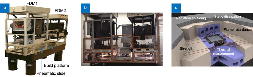
    Embedded electronics can greatly reduce the mass and assembly complexity due to the elimination of cabled interconnects and redundant electronics packaging. The ability to embed complex functioning components and electronics into 3D printed structures is very crucial for the small-satellite users who are looking to exploit 3DP in a limited space. NASA/GRC (National Aeronautics and Space Administration/Glenn Research Center) and America Makes have performed AM techniques to develop the embedded electronics used in the structures of spacecraft. A manufacturing platform, the multi3D system which integrates two FDM (fused deposition modeling) systems, a CNC (computer numerical control) router for micromachining and a precision dispenser for depositing conductive inks (as shown in Fig. 1), has been developed to produce 3D, multi-material, multifunctional devices (3D-printed CubeSat module) for addressing the requirements of aerospace applications. The system can embed wires and components on a multi-material substrate to provide mechanical, electronic, thermal and electromagnetic functionality, and making conformal structures with integrated electronics. Figure 2 illustrates the process flow of the multi3D system and fabricated parts using the platform. A CubeSat Trailblazer integrated a 3D-printed structure and the embedded electronics has been successfully launched in 20139, 14, 17-20.

    (a, b) Photograph of the multi3D system. (c) Schematic of a fabrication example9, 14

    Figure 1.(a, b) Photograph of the multi3D system. (c) Schematic of a fabrication example9, 14

    (a) Process flow of the multi3D system. (b) Fabricated parts9, 14

    Figure 2.(a) Process flow of the multi3D system. (b) Fabricated parts9, 14

    Figure 3 demonstrated the fabrication procedure of a fully encapsulated capacitive sensor. This study provides a proof of concept for advanced fully encapsulated 3D printable devices. It also verified the utility of fully embedded bulk conductors interconnect21.

    Fabrication procedure of fully encapsulated capacitive sensor with 3D printing. (a) Polycarbonate (PC) substrate with recesses designed for all electronic components. (b) Components arranged in in the PC substrate. (c) Electrical components with corresponding embedded wiring. (d) Completed capacitive sensor with fully embedded wiring, diodes, LEDs, resistors, and a microcontroller21

    Figure 3.Fabrication procedure of fully encapsulated capacitive sensor with 3D printing. (a) Polycarbonate (PC) substrate with recesses designed for all electronic components. (b) Components arranged in in the PC substrate. (c) Electrical components with corresponding embedded wiring. (d) Completed capacitive sensor with fully embedded wiring, diodes, LEDs, resistors, and a microcontroller21

    A shoe insole with embedded pressure and temperature sensing circuitry, with wireless communications chip for data transmission was fabricated by multi-material 3D printing, shown in Fig. 4. Using a hybrid 3D printing process, multi-layer tactile sensors including insulating layers and sensing elements have been built. This process enables building a sensor body layer by layer, prints sensing elements onto the surface of the body, and builds additional layers. With the combination of ink jet, aerosol jet and extrusion print heads, the deposited material can ranges from one to tens of thousands cps with a wide range of solvents. The case demonstrated the feasibility of fabricating an electronically functional object through 3D printing22.

    (a) Printed wireless pressure and temperature sensor within a shoe's insole. (b) Pressure and temperature data obtained through wireless communication from the printed insole22

    Figure 4.(a) Printed wireless pressure and temperature sensor within a shoe's insole. (b) Pressure and temperature data obtained through wireless communication from the printed insole22

    Figure 5 shows a 3D "smart cap" with an embedded inductor–a wireless passive sensor, which has been demonstrated to monitor the quality of liquid food wirelessly. The 3D structures including both supporting and sacrificial structures are constructed with a resolution of 30 μm using the FDM technology equipped with a multiple-nozzle system. After removing the sacrificial materials, silver particles suspensions are injected subsequently and solidified as the metallic elements/interconnects. This may be the first demonstration of a comprehensive manufacture process for printing 3D additive polymer with liquid metal paste filling for the use of potential applications12.

    Fabrication process of 3D "smart cap" with an embedded inductor–a wireless passive sensor12. (a) 3D fabrication process with embedded and electrically conductive structures. (b) 3D microelectronics components, including parallel-plate capacitors, solenoid-type inductors, and meandering-shape resistors. (c) A 3D LC tank, which is formed by combining a solenoid-type inductor and a parallel-plate capacitor. (d) A wireless passive sensor demonstration of a "smart cap", containing the 3D-printed LC-resonant circuit. (e) A smart cap with a half-gallon milk package, and the cross-sectional schematic diagram. (f) Sensing principle with the equivalent circuit diagram

    Figure 5.Fabrication process of 3D "smart cap" with an embedded inductor–a wireless passive sensor12. (a) 3D fabrication process with embedded and electrically conductive structures. (b) 3D microelectronics components, including parallel-plate capacitors, solenoid-type inductors, and meandering-shape resistors. (c) A 3D LC tank, which is formed by combining a solenoid-type inductor and a parallel-plate capacitor. (d) A wireless passive sensor demonstration of a "smart cap", containing the 3D-printed LC-resonant circuit. (e) A smart cap with a half-gallon milk package, and the cross-sectional schematic diagram. (f) Sensing principle with the equivalent circuit diagram

    A commercial 3Dn-300 multi-material printer from nScrypt Inc. has been utilized to fabricate a fully embedded low-profile antenna. The 3D printer includes dual deposition heads allowing two different kinds of materials to be dispensed. The thermoplastic stock is dispensed from one head through a filament extrusion process to print the dielectric components. While the other head prints the ink/paste is printed from the other head with feature sizes of as small as 20 μm to build the conductive elements23.

    A hybrid 3D printing process integrating stereolithography (SL) and direct print (DP) was adopted to produce functional, monolithic 3D structures with embedded electronics. The hybrid SL/DP system (as shown in Fig. 6) consists of a 3D Systems SL 250/50 machine and an nScrypt micro-dispensing pump integrated within the SL machine through orthogonally-aligned linear translation stages. The substrate/mechanical structure was fabricated by SL while interconnections were made by DP conductive inks. A process was developed to fabricate a 3D electronic device using the hybrid SL/DP machine with the requirement of multiple starts and stops of the SL process, removing the uncured resin from the SL substrate, inserting active and passive electronic components, and DP and laser curing of the conductive traces. By curing the conductive traces in situ, the construction of monolithic 3D structural electronic devices can be performed without removal of the device from the machine during fabrication. Functional 2D and 3D 555 timer circuits have been fabricated by the hybrid 3D printing system combined with the proposed process24. Jang et al. also presented a 3D circuit device fabrication by the hybrid process of SL and DW technologies. A custom-made SL system was adopted instead of a commercial SL machine25.

    (a) Schematic of the hybrid SL/DP system. (b~d) Fabricated 3D 555 timer circuits packaged within SL substrates24

    Figure 6.(a) Schematic of the hybrid SL/DP system. (b~d) Fabricated 3D 555 timer circuits packaged within SL substrates24

    3D structural electronics

    A hybrid technology combined with direct-write/cure (DWC) and projection microstereolithography (PμSL) has been utilized to make 3D structural electronics. A PμSL process was applied to build the 3D structures, and the conductive tracks was produced by the combination of DWC with CNT/polymer nanocomposites, which may capacitate a new generation of inexpensive 3D structural electronics in the field of consumer, defense, and medical electronics. The technology of hybrid manufacturing combined with AM technologies will offer capabilities of fully 3D, high-resolution, multimaterial and large-area fabrication as well as requiring only ambient processing conditions (no clean room, vacuum or high temperature environment required). Figure 7 demonstrated the hybrid 3D printing process and the fabricated 3D structural electronics10.

    The hybrid 3D printing process and fabricated 3D structural electronics10. (a) Bottom insulating structure. (b) "U" shape wire. (c) Top insulating layer. (d) Wires on top surface. (e) PμSL of the bottom insulating structure. (f) DWC of the "U" shape wire. (g) PμSL of the top insulating structure. (h) DWC of wires on the top surface. (i) Fabricated 3D structural electronics with embedded wires

    Figure 7.The hybrid 3D printing process and fabricated 3D structural electronics10. (a) Bottom insulating structure. (b) "U" shape wire. (c) Top insulating layer. (d) Wires on top surface. (e) PμSL of the bottom insulating structure. (f) DWC of the "U" shape wire. (g) PμSL of the top insulating structure. (h) DWC of wires on the top surface. (i) Fabricated 3D structural electronics with embedded wires

    Disadvantages in the manufacturing process of printed circuit board include complexity, time consuming, higher cost, and limited product formation as the printed circuit board must be included. In order to get over these disadvantages, Jiang et al. reported a hybrid process using stereolithography and direct writing (DW) to fabricate 3D circuit devices. The insulated structures of circuit boards having high precision were fabricated using SL. Furthermore, the circuits were made on the several layers using DW25. Lopes et al. also presented a similar manufacturing system using SL and DW technologies for the fabrication of 3D structural electronics24.

    The integration of SL in combination with both microdispensing (nozzle deposition) and pick-and-place technology (component insertion) can produce dielectric substrates of intricately-detailed, complex shape where miniature cavities are used for the integration of press-fit electronic components. Printed conductive traces serve as electrical connections deposited by an integrated micro-dispensing system within the SL system and this combination of fabrication technologies stands to revolutionize the integration of electronics within mechanical structures as "3D structural electronics". Wicker and MacDonald demonstrated the development of multiple material and multiple technology SL systems capable of manufacturing multiple material structures with mechanical, electrical, and biochemical functionality. Some functional objects including multi-material tissue engineered implants, multi-material micro-scale parts, 3D structural electronics, have been successfully fabricated. Contamination issues associated with using multiple viscous materials in a single build, throughput, and limited materials as well as conductive inks with low-temperature curing capabilities remain still a challenging. Figure 8 shows some examples of printed 3D structural electronics18, 24.

    Examples of printed 3D structural electronics18. (a) A gaming die which includes a microcontroller and accelerometer. (b, c) A magnetometer system with microprocessor and orthogonal Hall Effect sensors

    Figure 8.Examples of printed 3D structural electronics18. (a) A gaming die which includes a microcontroller and accelerometer. (b, c) A magnetometer system with microprocessor and orthogonal Hall Effect sensors

    Stretchable electronics

    With the development of electronics, progresses in manufacturing techniques have promoted the development in the aspects of smaller, faster, more efficient. So far, the main focus has been on rigid electronics. However, recent interest in devices such as wearable electronics and soft robotics has led to an whole new set of electronic devices–stretchable electronics. These new devices require new manufacturing solutions to integrate heterogeneous soft functional materials. 3D printing can be harnessed to print electronics on stretchable and flexible bio-compatible "skins" with integrated circuitry that can conform to irregularly-shaped mounting surfaces.

    Muth et al. reported a method of embedded 3D printing (e-3DP) for the fabrication of strain sensors, as shown in Fig. 9. In this method, a viscoelastic ink is extruded into an elastomeric reservoir via a deposition nozzle. The ink is used as a resistive sensing element, while the reservoir form the matrix material. A capping (filler fluid) layer is used to fill the void space formed in the process of the nozzle translating through the reservoir. Finally, a monolithic part was formed by the co-cure of both the reservoir and filler fluid, which covered and keep the embedded conductive ink fluid. The e-3DP can create soft sensors in a highly programmable and seamless manner. In order to enable e-3DP, a multicomponent materials system composed of an ink, reservoir, and filler fluid was developed. The above method that for building highly stretchable sensors by e-3DP opens new approaches for manufacturing soft functional devices for wearable electronics, human/machine interfaces, soft robotics, and so on11.

    Schematic illustration of the embedded 3D printing (e-3DP) process and printed stretchable electronics11. (a) Schematic illustration of the e-3DP process. (b) Photograph of a glove with embedded strain sensors produced by e-3DP. (c) Photograph of a three-layer strain and pressure sensor in the stretched state

    Figure 9.Schematic illustration of the embedded 3D printing (e-3DP) process and printed stretchable electronics11. (a) Schematic illustration of the e-3DP process. (b) Photograph of a glove with embedded strain sensors produced by e-3DP. (c) Photograph of a three-layer strain and pressure sensor in the stretched state

    The ability of printing integrated circuits on the flexible substrate enables the electronic devices with conformity, lightweight structure and shock-resistant construction, which are challenging to be achieved by using rigid substrates such as semiconductor wafers and glass plates. Bijadi et al. have successfully tested the feasibility of a syringe extrusion-based 3D printing process to print stretchable embedded electronics through the use of SS-26S conductive silicone on flexible non-conductive silicone substrates. Instead of merely using the conductive silicone traces as flexible interconnects, this method used the conductive material for creating complete circuitry with SMT components and embedded microcontrollers26. Vatani et al. presented a hybrid manufacturing process including direct print/cure (DPC) and projection-based stereolithography for stretchable tactile sensors. The fabrication process of the tactile sensor (shown in Fig. 10) includes building the sensor body, printing sensing elements on the body surface, and building some additional layers to cover the cured sensing elements27. The developed 3D printable stretchable sensing material is a photocurable and stretchable liquid resin filled with multi-walled carbon nanotubes (MWNTs).

    Fabricated stretchable tactile sensor using integrated PSL and DP processes27. (a) An example (partial sphere) of 3D structure built in the PSL system. (b) Printed sensing elements using the DP process on the insulating layers built in the PSL system. (c) Final sensor with two sensing layers. (d) Deformed sensor

    Figure 10.Fabricated stretchable tactile sensor using integrated PSL and DP processes27. (a) An example (partial sphere) of 3D structure built in the PSL system. (b) Printed sensing elements using the DP process on the insulating layers built in the PSL system. (c) Final sensor with two sensing layers. (d) Deformed sensor

    Other electronic/electrical products and related technologies

    3D printing possesses the ability of creating complex and conformal electronics integrated within a manufactured product. The Aerosol Jet printing from Optomec has been demonstrated the ability of building the functional antennae on the conformal 3D printing substrates. The whole printing process accurately controls the location, geometry and thickness of the deposit and produces a smooth mirror-like surface finish to insure optimum antenna performance. Some kinds of mobile device antennas, such as the LTE, NFC, GPS, Wifi, WLAN, and BT, have been printed through the Aerosol Jet process. And the performance of such antennas tested by a cell phone component supplier is in the same level with other production methods. For now, the Aerosol Jet technology has been using for the mass production of printed 3D conformal electronics in the application of antenna and sensor. As can been seen that a hybridized DW/AM process presents great potential for creating antennas with 3-dimensional structure. Figure 11 demonstrated 3D printed electronics using Aerosol Jet printing process28-30.

    3D printed electronics using Aerosol Jet printing from Optomec28-30. (a) 3D MID demonstrator. (b) 3D MID with integrated sensor.(c) Printed conformal electronics (curve). (d) Printed conformal electronics (dome). (e) Printed conformal electronics (dome). (f) Sub-mm length scale, custom made 3D metal-dielectric

    Figure 11.3D printed electronics using Aerosol Jet printing from Optomec28-30. (a) 3D MID demonstrator. (b) 3D MID with integrated sensor. (c) Printed conformal electronics (curve). (d) Printed conformal electronics (dome). (e) Printed conformal electronics (dome). (f) Sub-mm length scale, custom made 3D metal-dielectric

    Aerosol Jet printing process has the ability to print conformal interconnects on 3D surfaces eliminating the need for wire bonding – for example printing electrical connections on 3D stacked die or for LED chip fabrication. Runge showed Leg prosthesis part produced from PLA (Polylactic Acid) via FDM showing complex non-planar surfaces, with surface-integrated strain gauge sensors produced by Aerosol Jet TM printing and conductive paths deposited via micro-dispensing, both using the modular manufacturing platform. The structural elements of this leg prosthesis shaft were produced via the FDM process from PLA, a thermoplastic polymer. Its functionalization relies on a surface-integrated strain gauge realized via Aerosol Jet printing. The conductive paths that lead across the part as well as the contact pads at their end were deposited through micro-dispensing. The material of the resistive sensor is a silver based ink, while interconnects and contact pads are made from silver particle-filled epoxy, as shown in Fig. 1231.

    Leg prosthesis part produced by FDM and Aerosol Jet printing31

    Figure 12.Leg prosthesis part produced by FDM and Aerosol Jet printing31

    The first multi-material 3D electronics printer in the world, named as Voxel8, provides an all-in-one, desktop solution for designing and prototyping next generation 3D electronic devices. Therefore, it has been regarded as a disruptive manufacture platform with the capabilities of printing embedded electronics. It enables prototyping of 3D electronic devices by the method of co-printing both thermoplastics and a highly conductive silver ink, which can be printed and cured at ambient temperature without the need for thermal annealing. Figure 13 demonstrates Voxel8 and some printed products32.

    Voxel8 and some printed products32. (a, b) Photograph of Voxel8 3D printer. (c) Printed unmanned aerial vehicle. (d) Printed antenna (dome). (e) Printed wearable device

    Figure 13.Voxel8 and some printed products32. (a, b) Photograph of Voxel8 3D printer. (c) Printed unmanned aerial vehicle. (d) Printed antenna (dome). (e) Printed wearable device

    Prospect, challenges and future trends

    3D printing is disrupting the design and manufacture of electronic products. Functionalities of the devices/products fabricated by 3D printing can be significantly expanded by incorporating electronic components, such as sensors and circuits, in predetermined cavities within fabricated structures. 3D printed objects include not only traditional mechanical characteristics, but also embedded optical and electrical functions, such as sensor; all complex structures are difficult to produce with existing manufacturing methods. Many emerging and innovative products, such as embedded electronics, 3D structural electronics, conformal electronics, stretchable electronics, etc., have been fabricated using the technologies. 3D printing electronics has been considered as the next frontier in AM. Optomec has developed a high volume printing solution for the production of 3D antenna and 3D sensors that are tightly integrated with an underlying product ranging from smartphones to industrial components. It can be utilized for high volume printing of conformal sensors and antennas directly onto preformed 3D structures. Complex electronics can be 3D printed at micron resolution which will enable cheaper smartphones and medical gadgets. Aerosol Jet 3D micro-structure printing is capable of ultra-high resolutions with lateral features sizes of 10 μm and aspect ratios of more than 100:1 33-37.

    The conductivity is still one of the major difficulties in both 3D printed electronics and general 2D printed electronics because of the poor conductivity of ink caused by the low curing temperature due to the limitation of substrate material such as cardboard, polymers. More and more challenges in the fields of material types and processing challenges in the process of printing from 2D electronics to 3D integrated objects. Therefore, the compatible material sets should be explored and created to provide the adequate functionality and manufacturability for the product invention by designers. Besides, the adhesion between the materials is also a big issue, because the conductive materials would be stripped from the substrate with a poor adhesion. This is especially important case for traces that are embedded within a print and not on the surface because repair is impossible after a circuit is embedded.

    In order to make electronics with 3D printing, new processes should be developed to possess the ability of depositing broader types of materials. To date, there are several solutions which have the ability to fabricate multifunctional 3D structures or products with embedded functional systems. Compared to other methods, the hybrid process combining FDM and direct print/writing shows higher applied potential, more flexibility. Material jetting systems seem currently to be the most successful multi-material 3D printing process among AM technologies. To date, fabrication of true 3D multiple material polymeric components using material jetting processes has been demonstrated. Currently, material jetting of polymers appears to be the nearest approximation to this vision that is currently available: The combination of high resolution, controlled material deposition with the possibility of photo polymerization, which allows immediate solidification of the material after printing and thus facilitates deposition of materials with different functional or structural roles directly besides each other, provides the foundation for effectively printing a structural electronics system directly. Multi-material and multi-scale 3D printing will be the most promising solutions.

    More and more 3D printed functional electronics and products with electronics will be fabricated. 3D printing electronic technology provides a powerful tool for innovative product development, and extends 3D printing multiple functionalities. Significant advances in 3D printing electronics have been accomplished in the recent years. However, there is still a long way to go for 3D printed functional electronics and products as well as their industrial-level applications. Further potentials of 3D printing electronics need still to be explored and investigated.

    Acknowledgements

    We are grateful for financial supports from the National Natural Science Foundation of China (51775288).

    Competing interests

    The authors declare no competing financial interests.

    References

    [1] I Gibson, D W Rosen, B Stucker . Additive manufacturing technologies(2010).

    [2] B Derby. Printing and prototyping of tissues and scaffolds. Science, 338, 921-926(2012).

    [3] J A Lewis, B Y Ahn. Device fabrication: Three-dimensional printed electronics. Nature, 518, 42-43(2015).

    [4] Y L Kong, I A Tamargo, H Kim, B N Johnson, M K Gupta et al. 3D printed quantum dot light-emitting diodes. Nano Lett, 14, 7017-7023(2014).

    [5] H Lan. Active mixing nozzle for multimaterial and multiscale three-dimensional printing. J Micro Nano-Manuf, 5, 040904(2017).

    [6] X Zheng, W Smith, J Jackson, B Moran, H Cui et al. Multiscale metallic metamaterials. Nature Mater, 15, 1100-1106(2016).

    [7] M Vaezi, H Seitz, S Yang. A review on 3D micro-additive manufacturing technologies. Int J Adv Manuf Technol, 67, 1721-1754(2013).

    [8] X Y Tian, L X Yin, D C Li. Current situation and trend of fabrication technologies for three-dimensional metamaterials. Opto-Electron Eng, 44, 69-76(2017).

    [9] D Espalin, D. W Muse, E MacDonald, R B Wicker. 3D Printing multifunctionality: structures with electronics. Int J Adv Manuf Technol, 72, 963-978(2014).

    [10] Y Lu, M Vatani, J W Choi. Direct-write/cure conductive polymer nanocomposites for 3D structural electronics. J Mech Sci Technol, 27, 2929-2934(2013).

    [11] J T Muth, D M Vogt, R L Truby, Y Mengüç, D B Kolesky et al. Embedded 3D printing of strain sensors within highly stretchable elastomers. Adv Mater, 26, 6307-6312(2014).

    [12] S Y Wu, C Yang, W Hsu, L Lin. 3D-printed microelectronics for integrated circuitry and passive wireless sensors. Microsys Nanoeng, 1, 15013(2015).

    [13] K Sun, T S Wei, B Y Ahn, J Y Seo, S J Dillon et al. 3D Printing of interdigitated Li-Ion microbattery architectures. Adv Mater, 25, 4539-4543(2013).

    [14] D Lehmhus, C Aumund-Kopp, F Petzoldt, D Godlinskic, A Haberkorn et al. Customized smartness: a survey on links between additive manufacturing and sensor integration. Procedia Tech, 26, 284-301(2016).

    [15] C Ladd, J H So, J Muth, M D Dickey. 3D printing of free standing liquid metal microstructures. Adv Mater, 25, 5081-5085(2013).

    [16] V A Lifton, G Lifton, S Simon. Options for additive rapid prototyping methods (3D printing) in MEMS technology. Rapid Prototyping J, 20, 403-412(2014).

    [17] E MacDonald, R Wicker. Multiprocess 3D printing for increasing component functionality. Science, 353, aaf2093(2016).

    [18] R B Wicker, E W MacDonald. Multi-material, multi-technology stereolithography. Virtual Phys Prototyping, 7, 181-194(2012).

    [19] Kief C J, Aarestad J, Macdonald E, Shemelya C, Roberson D A et al. Printing multi-functionality: additive manufacturing for CubeSats. In AIAA SPACE 2014 Conference and Exposition, AIAA SPACE Forum 4193 (AIAA, 2014). https://doi.org/10.2514/6.2014-4193

    [20] M Liang, C Shemelya, E MacDonald, R Wicker, H Xin. 3D printed microwave patch antenna via fused deposition method and ultrasonic wire mesh embedding technique. IEEE Antennas Wireless Propag Lett, 14, 1346-1349(2015).

    [21] C Shemelya, F Cedillos, E Aguilera, D Espalin, D Muse et al. Encapsulated copper wire and copper mesh capacitive sensing for 3-D printing applications. IEEE Sens J, 15, 1280-1286(2015).

    [22] Ready S, Whiting G, Ng T N. Multi-material 3D printing. In NIP & Digital Fabrication Conference, 2014 International Conference on Digital Printing Technologies 120–123 (2014)..

    [23] P Pa, Z Larimore, P Parsons, M Mirotznik. Multi-material additive manufacturing of embedded low-profile antennas. Electron Lett, 51, 1561-1562(2015).

    [24] A J Lopes, E MacDonald, R B Wicker. Integrating stereolithography and direct print technologies for 3D structural electronics fabrication. Rapid Prototyping J, 18, 129-143(2012).

    [25] S H Jang, S T Oh, I H Lee, H C Kim, H Y Cho. 3-Dimensional circuit device fabrication process using stereolithography and direct writing. Int J Precis Eng Man, 16, 1361-1367(2015).

    [26] Bijadi S. Feasibility of additive manufacturing method for developing stretchable and flexible embedded circuits (University of Minnesota, Minneapolis, USA, 2014). .

    [27] M Vatani, Y Lu, E D Engeberg, J W Choi. Combined 3D printing technologies and material for fabrication of tactile sensors. Int J Precis Eng Man, 16, 1375-1383(2015).

    [28] Hedges M. 3D Printed Electronics via Aerosol Jet (Neotech, 2014). .

    [29] Hedges M. Optomec. https://www.optomec.com (2017). . https://www.optomec.com

    [30] Cai F, Pavlidis S, Papapolymerou J, Chang Y H, Wang K et al. Aerosol jet printing for 3-D multilayer passive microwave circuitry. In IEEE European Microwave Conference (IEEE, 2014) . http://do.org/10.1109/EuMC.2014.6986483

    [31] Runge D. 3D-Printing und gedruckte Elektronik für die Medizintechnik (University of Applied Science Bremerhaven, Bremen Area, Germany, 2016). .

    [32] Voxel8. https://www.voxel8.com (2017). . https://www.voxel8.com

    [33] Dickey M. Liquid metals for soft and stretchable electronics. In Stretchable Bioelectronics for Medical Devices and Systems. Microsystems and Nanosystems (Springer, Cham, 2016) . https://doi.org/10.1007/978-3-319-28694-5_1

    [34] M T Rahman, A Rahimi, S Gupta, R Panata. Microscale additive manufacturing and modeling of interdigitated capacitive touch sensors. Sensor Actuat A-Phys, 248, 94-103(2016).

    [35] J Donnell, M Kim, H Yoon. A review on electromechanical devices fabricated by additive manufacturing. ASME J Manuf Sci E-T, 139, 010801(2017).

    [36] B Thompson, H S Yoon. Aerosol-printed strain sensor using PEDOT: PSS. IEEE Sens J, 13, 4256-4263(2013).

    [37] K E Madden, A D Deshpande. On integration of additive manufacturing during the design and development of a rehabilitation robot: a case study. ASME J Mech Des, 137, 111417(2015).

    Bingheng Lu, Hongbo Lan, Hongzhong Liu. Additive manufacturing frontier: 3D printing electronics[J]. Opto-Electronic Advances, 2018, 1(1): 170004
    Download Citation