• Journal of Semiconductors
  • Vol. 42, Issue 3, 031101 (2021)
Ying Zhu, Yongli He, Shanshan Jiang, Li Zhu, Chunsheng Chen, and Qing Wan
DOI: 10.1088/1674-4926/42/3/031101 Cite this Article
Ying Zhu, Yongli He, Shanshan Jiang, Li Zhu, Chunsheng Chen, Qing Wan. Indium–gallium–zinc–oxide thin-film transistors: Materials, devices, and applications[J]. Journal of Semiconductors, 2021, 42(3): 031101 Copy Citation Text show less
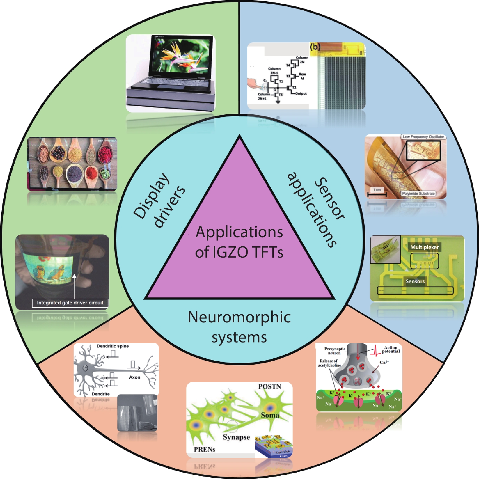
(Color online) Some important applications of IGZO-based TFTs[11, 20, 34–37, 46–48].
Fig. 1. (Color online) Some important applications of IGZO-based TFTs[11, 20, 3437, 4648].
(Color online) Carrier transport paths of (a) crystalline, (b) amorphous post-transition-metal oxide semiconductors[3].
Fig. 2. (Color online) Carrier transport paths of (a) crystalline, (b) amorphous post-transition-metal oxide semiconductors[3].
(Color online) A time axis diagram of the development of the IGZO-based TFT[1–3, 11, 20, 36, 44, 57, 62].
Fig. 3. (Color online) A time axis diagram of the development of the IGZO-based TFT[13, 11, 20, 36, 44, 57, 62].
(Color online) Schematic diagrams of the device structures with (a) bottom gate, (b) top gate, (c) double gate, (d) vertical and (e) multiple gates.
Fig. 4. (Color online) Schematic diagrams of the device structures with (a) bottom gate, (b) top gate, (c) double gate, (d) vertical and (e) multiple gates.
(Color online) (a) Schematic diagram of the bottom-gate coplanar homojunction a-IGZO device structure. (b, c) Transfer and output curves of the device, respectively[75].
Fig. 5. (Color online) (a) Schematic diagram of the bottom-gate coplanar homojunction a-IGZO device structure. (b, c) Transfer and output curves of the device, respectively[75].
(Color online) (a) Schematic diagram of the top-gate a-IGZO-based TFT structure and the major processing steps, respectively. (c, d) Transfer and output curves of the a-IGZO-based TFT, respectively[74].
Fig. 6. (Color online) (a) Schematic diagram of the top-gate a-IGZO-based TFT structure and the major processing steps, respectively. (c, d) Transfer and output curves of the a-IGZO-based TFT, respectively[74].
(Color online) Schematic diagrams of the structures of (a) single-gate and (b) dual-gate TFT, respectively. (c, d) Transfer and output curves of the single-gate device, respectively. (e, f) Transfer and output curves of the dual-gate device, respectively[66].
Fig. 7. (Color online) Schematic diagrams of the structures of (a) single-gate and (b) dual-gate TFT, respectively. (c, d) Transfer and output curves of the single-gate device, respectively. (e, f) Transfer and output curves of the dual-gate device, respectively[66].
(Color online) (a, b) Schematic diagrams of the vertical IGZO-based TFT structures. (c, d) Carriers transferred in the planar and vertical TFTs with cracks in the IGZO thin film, respectively[70].
Fig. 8. (Color online) (a, b) Schematic diagrams of the vertical IGZO-based TFT structures. (c, d) Carriers transferred in the planar and vertical TFTs with cracks in the IGZO thin film, respectively[70].
(Color online) Schematic diagram of the IGZO-based neuron TFTs with multi-gate structure[72].
Fig. 9. (Color online) Schematic diagram of the IGZO-based neuron TFTs with multi-gate structure[72].
(Color online) Pixel circuit of the AMLCD based on synchronized dual-gate a-IGZO-based TFTs[91].
Fig. 10. (Color online) Pixel circuit of the AMLCD based on synchronized dual-gate a-IGZO-based TFTs[91].
(Color online) (a) Schematic diagram of the measured dual-gate a-IGZO-based TFT structure. (b) Definition of the electrodes. (c) Transfer curves of the dual-gate a-IGZO-based TFT under primary gate operation with auxiliary gate voltage changing from –4 to 4 V. (d) Threshold voltage as a function of auxiliary gate voltage. (e) Structure of the pixel circuit[101].
Fig. 11. (Color online) (a) Schematic diagram of the measured dual-gate a-IGZO-based TFT structure. (b) Definition of the electrodes. (c) Transfer curves of the dual-gate a-IGZO-based TFT under primary gate operation with auxiliary gate voltage changing from –4 to 4 V. (d) Threshold voltage as a function of auxiliary gate voltage. (e) Structure of the pixel circuit[101].
(Color online) Conceptual architecture and flexible display panel with carry-free gate driver[117].
Fig. 12. (Color online) Conceptual architecture and flexible display panel with carry-free gate driver[117].
(Color online) Picture images of the display panels of large size, high-resolution and narrow bezel[62, 121, 122].
Fig. 13. (Color online) Picture images of the display panels of large size, high-resolution and narrow bezel[62, 121, 122].
(Color online) (a) A schematic diagram of the IGZO-based TFT structure. (b) The separation and collection process of the photo-generated carriers. (c) Photoresponse of the IGZO and PEDOT:PSS/SnOx/IGZO phototransistors as a function of the light wavelength[27].
Fig. 14. (Color online) (a) A schematic diagram of the IGZO-based TFT structure. (b) The separation and collection process of the photo-generated carriers. (c) Photoresponse of the IGZO and PEDOT:PSS/SnOx/IGZO phototransistors as a function of the light wavelength[27].
(Color online) (a) Schematic diagram of the a-IGZO-based TFT pressure sensor structure. (b) Transfer characteristics of the dual-gate TFT with different top-gate voltage[133].
Fig. 15. (Color online) (a) Schematic diagram of the a-IGZO-based TFT pressure sensor structure. (b) Transfer characteristics of the dual-gate TFT with different top-gate voltage[133].
(Color online) (a) Structure of the flexible extended-gate ISFET pH sensor. (b) Data graph of the drain current vs time[19].
Fig. 16. (Color online) (a) Structure of the flexible extended-gate ISFET pH sensor. (b) Data graph of the drain current vs time[19].
(Color online) (a) Schematic diagram of the IGZO-based TFT structure. (b) Transfer curves with different time under 50 ppm NO2 gas concentration. (c) Drain current vs time under 50 ppm NO2 gas concentration[137].
Fig. 17. (Color online) (a) Schematic diagram of the IGZO-based TFT structure. (b) Transfer curves with different time under 50 ppm NO2 gas concentration. (c) Drain current vs time under 50 ppm NO2 gas concentration[137].
(Color online) Schematic diagrams of the a-IGZO-based TFT pressure-sensing system and output curves[22].
Fig. 18. (Color online) Schematic diagrams of the a-IGZO-based TFT pressure-sensing system and output curves[22].
(Color online) Schematic diagram of an artificial synapse based on neuromorphic transistor.
Fig. 19. (Color online) Schematic diagram of an artificial synapse based on neuromorphic transistor.
(Color online) (a) Schematic diagram of the electric-double-layer (EDL) IGZO-based neuromorphic TFT structure. (b) Simple schematic diagram of an artificial synapse based on the IGZO-based TFT. (c) PPF ratio as a function of the time interval between the two stimuli spike. (d) EPSC amplitude gain as a function of spike frequency[161].
Fig. 20. (Color online) (a) Schematic diagram of the electric-double-layer (EDL) IGZO-based neuromorphic TFT structure. (b) Simple schematic diagram of an artificial synapse based on the IGZO-based TFT. (c) PPF ratio as a function of the time interval between the two stimuli spike. (d) EPSC amplitude gain as a function of spike frequency[161].
(Color online) (a, b) Schematic images of the top-gate IGZO-based neuromorphic TFTs with electrolyte gate dielectric. (c, d) EPSC as a function of pulse number and rate of the positive presynaptic spike trains, respectively[45].
Fig. 21. (Color online) (a, b) Schematic images of the top-gate IGZO-based neuromorphic TFTs with electrolyte gate dielectric. (c, d) EPSC as a function of pulse number and rate of the positive presynaptic spike trains, respectively[45].
(Color online) (a) Schematic diagram of sound location of the human brain. (b) Schematic picture of the IGZO neuromorphic device and neural network for the emulation of sound azimuth detection. (c) IPOSTN1 and IPOSTN2 when the sound comes from the right direction. (d) The ratio of IPOST2 and IPOST1 as a function of the sound azimuth[36].
Fig. 22. (Color online) (a) Schematic diagram of sound location of the human brain. (b) Schematic picture of the IGZO neuromorphic device and neural network for the emulation of sound azimuth detection. (c) IPOSTN1 and IPOSTN2 when the sound comes from the right direction. (d) The ratio of IPOST2 and IPOST1 as a function of the sound azimuth[36].
SubstrateStructure of the TFTμFE(cm2/(V·s)) Vth(V) SS (V/dec)Size (inch)ApplicationRef.
GlassDual-gate110.2413055LCD[118]
GlassInverted stagger932LCD[48]
GlassBottom gate153.20.480LCD[104]
GlassInverted bottom gate4.2±0.4–1.30.96±0.115AMLCD[12]
GlassBack channel etch7.351.6AMLED[100]
GlassStaggered bottom gate8.21.10.5812.1AMOLED[11]
18.451.040.73AMOLED[97]
GlassEtch stopper204.8AMOLED[103]
PolyimideStaggered bottom gate17.30.860.2111.7Flexible AMOLED[119]
PolyimideInverted staggered bottom gate11.61.60.253Flexible AMOLED[34]
PolyimideCoplanar10.250.340.22Flexible OLED[120]
Table 1. Display applications of the IGZO-based TFTs.
SubstrateStructure of the TFTμFE(cm2V–1s–1) Ion/IoffVth(V) SS (V/dec)ApplicationRef.
SiO2/Si Top gate18~1060.60.07Photoelectric sensor[145]
SiBottom gate10.82.30.34Phototransistor[131]
GlassBottom-gate31.08 × 1050.50.49Deep-ultraviolet phototransistor[146]
SiO2/Si Double gate6.515 × 1060.510.12PH sensor[136]
SiDouble gate41072.80.31PH sensor[126]
SiO2/Si Bottom gate7.58~1070.49Gas sensor[147]
Double gate13.82.9 × 1060.720.19Hybrid gas sensor[30]
GlassBottom gate121.39–1.920.24Temperature sensor[16]
Metal foilBottom gate21~1077.361.12Flexible thermal and pressure sensor[148]
PolyimideBack channel etch201071Flexible pressure sensor[149]
Polyethylene naphthalateBottom-gateBiosensor[19]
PolyethylenenaphthalateBottom-gate staggered10~1520.3Flexible X-Ray detector[150]
PolyimideBottom-gate inverted staggered13.340.87Flexible gas sensor[140]
Table 2. Sensor applications of the IGZO-based TFTs.
Ying Zhu, Yongli He, Shanshan Jiang, Li Zhu, Chunsheng Chen, Qing Wan. Indium–gallium–zinc–oxide thin-film transistors: Materials, devices, and applications[J]. Journal of Semiconductors, 2021, 42(3): 031101
Download Citation