
Ying Zhu, Yongli He, Shanshan Jiang, Li Zhu, Chunsheng Chen, Qing Wan. Indium–gallium–zinc–oxide thin-film transistors: Materials, devices, and applications[J]. Journal of Semiconductors, 2021, 42(3): 031101
- Journal of Semiconductors
- Vol. 42, Issue 3, 031101 (2021)
Abstract
1. Introduction
Metal oxide semiconductor thin-film transistors (TFTs), especially indium–gallium–zinc–oxide (IGZO)-based TFTs, have received considerable interest since Nomura et al. reported the first amorphous IGZO (a-IGZO) based TFT in 2004. Before the invention of the first a-IGZO-based TFT, the crystalline IGZO materials were first reported as early as 1985[
Several well-known display companies (e.g., Sharp, Samsung Electronics, and LG Electronics) have demonstrated that IGZO-based TFTs have many potential applications in liquid crystal displays (LCDs), organic light emitting diodes (OLEDs) display and electronic paper displays[
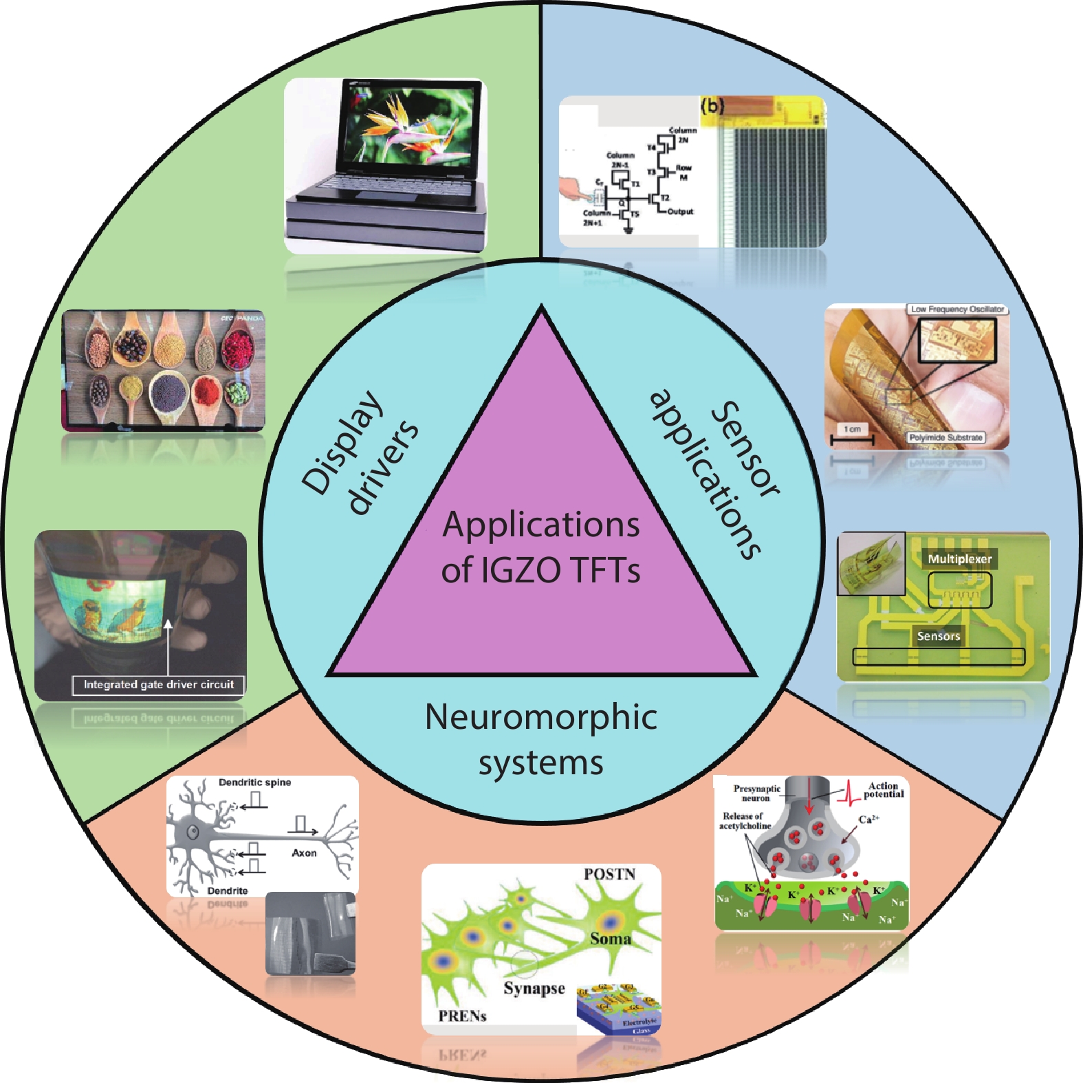
![]()
Figure 1.(Color online) Some important applications of IGZO-based TFTs[
With the rapid development of IGZO-based TFTs in various aspects of our life, especially in the field of display, a large number of studies based on the IGZO-based TFTs have been reported. Thus, this article aims to review the recent progress and the major trends in the field of IGZO-based TFTs. In this paper, we review the materials, devices and applications of IGZO-based TFTs. First, the history, electron travelling orbitals and deposition methods of the IGZO thin film are introduced. Second, we introduce the traditional devices and the new-concept device structures. Third, we comprehensively discuss the main applications, including display drivers, sensor applications and neuromorphic systems using IGZO-based TFTs. Finally, our conclusions and the outlook for IGZO-based TFTs are discussed.
2. IGZO materials and TFTs
2.1. IGZO materials
Crystalline IGZO materials were first discovered by Kimizuka et al. in 1985[
The electron travelling orbitals of oxide semiconductors are different from covalent semiconductors. Covalent semiconductors (e.g., silicon) possess carrier transport paths of directive sp3 orbitals[
![]()
Figure 2.(Color online) Carrier transport paths of (a) crystalline, (b) amorphous post-transition-metal oxide semiconductors[
Many methods have been proposed to deposit IGZO thin films. The most commonly used method is sputtering because it is compatible with uniform deposition on the large surface with low cost[
2.2. IGZO-based TFTs
The first concept of thin-film transistors (TFTs) was patented as early as the 1930s[
![]()
Figure 3.(Color online) A time axis diagram of the development of the IGZO-based TFT[
Many possible device structures for IGZO-based TFTs are shown in Fig. 4[
![]()
Figure 4.(Color online) Schematic diagrams of the device structures with (a) bottom gate, (b) top gate, (c) double gate, (d) vertical and (e) multiple gates.
In IGZO-based TFTs, source/drain electrodes, gate electrode, gate dielectric and IGZO semiconductor channel material are used in the TFT structures. Electrodes are usually composed of metal materials, high conductive metal oxides and new materials such as graphene[
Sato et al. presented a bottom-gate type coplanar homojunction a-IGZO-based TFT[
![]()
Figure 5.(Color online) (a) Schematic diagram of the bottom-gate coplanar homojunction a-IGZO device structure. (b, c) Transfer and output curves of the device, respectively[
Zhang et al. proposed a self-aligned top-gate a-IGZO-based TFT with a thickness of 8.62 nm SiO2 as gate dielectric[
![]()
Figure 6.(Color online) (a) Schematic diagram of the top-gate a-IGZO-based TFT structure and the major processing steps, respectively. (c, d) Transfer and output curves of the a-IGZO-based TFT, respectively[
In the dual-gate structure, the top gate and bottom gate are together used to modulate the channel carrier concentration and further control the electrical performance of the device, such as the turn-on voltage, the threshold voltage and the field-effect mobility, through applying voltage to the bottom and top-gate electrodes[
![]()
Figure 7.(Color online) Schematic diagrams of the structures of (a) single-gate and (b) dual-gate TFT, respectively. (c, d) Transfer and output curves of the single-gate device, respectively. (e, f) Transfer and output curves of the dual-gate device, respectively[
Vertical structure devices can offer ultrashort channel with high current. Furthermore, the ultrashort channel enables the device to resist mechanical stress, which is especially important for flexible devices[
![]()
Figure 8.(Color online) (a, b) Schematic diagrams of the vertical IGZO-based TFT structures. (c, d) Carriers transferred in the planar and vertical TFTs with cracks in the IGZO thin film, respectively[
In 2017, IGZO-based neuron TFTs with multiple in-plane gate electrodes were reported by our group[
![]()
Figure 9.(Color online) Schematic diagram of the IGZO-based neuron TFTs with multi-gate structure[
3. Applications
IGZO-based TFTs have been applied in many areas, such as display drivers, sensors and neuromorphic systems[
3.1. Display drivers
Hydrogenated amorphous silicon (a-Si:H) and low-temperature polysilicon (LTPS) have been widely used in practical displays. However, the electron mobility of a-Si:H is usually low (1.0 cm2/(V·s)) and the TFTs are unstable under stress and illumination[
3.1.1. LCDs
LCDs are a relatively mature technology and are used in display panels, such as smart phone displays, tablet personal computers and televisions. The trends of LCDs are high resolution (7680 × 4320 pixels), ultra-high pixel density of over 300-ppi (pixels per inch) and refresh rate of 240 Hz or higher. To follow these trends, smaller and faster TFTs are required. Consequently, a-IGZO-based TFTs are considered as an advanced method to achieve the high pixel density on a large panel size, due to their high mobility and small size. For example, Baek et al. reported a dual-gate synchronized a-IGZO-based TFT for the application of an active-matrix liquid crystal display (AMLCD)[
![]()
Figure 10.(Color online) Pixel circuit of the AMLCD based on synchronized dual-gate a-IGZO-based TFTs[
3.1.2. OLEDs
OLEDs driven by a-IGZO-based TFTs are still in the development stage and they have not been put into the display market on a large scale. For further development, crucial problems such as device stability, imaging uniformity and yield[
![]()
Figure 11.(Color online) (a) Schematic diagram of the measured dual-gate a-IGZO-based TFT structure. (b) Definition of the electrodes. (c) Transfer curves of the dual-gate a-IGZO-based TFT under primary gate operation with auxiliary gate voltage changing from –4 to 4 V. (d) Threshold voltage as a function of auxiliary gate voltage. (e) Structure of the pixel circuit[
3.1.3. Flexible displays
Flexible IGZO-based TFTs are capable for use as flexible displays, due to the unique advantages such as light-weight substrates[
Most TFT gate drivers integrated on the display panel use carry signals between the stages. However, in the flexible display the error of the stressed stages is accumulated through the carry signals when the display panel is bent. This problem will probably lead to the failure of the image refresh. To deal with this problem, Kim et al. reported a carry-free gate driver for flexible displays using a-IGZO-based TFTs[
![]()
Figure 12.(Color online) Conceptual architecture and flexible display panel with carry-free gate driver[
Table 1 shows the recent studies of the display applications driven by the a-IGZO-based TFTs. This table shows the substrate, structure, electrical properties of the a-IGZO-based TFTs, the size of the display panel and the specific application.
Nowadays, a-IGZO-based TFTs have attracted considerable attention thanks to their large-size, high-resolution and narrow-bezel display applications. Fig. 13 shows this progress in display applications. For example, China Star Optoelectronics Technology (CSOT) developed an 85-inch 8k4k LCD driven by the IGZO-based TFTs. The large-size LCD panel is shown in Fig. 13(a)[
![]()
Figure 13.(Color online) Picture images of the display panels of large size, high-resolution and narrow bezel[
3.2. Sensor applications
Sensors can detect the light, force, voice, gas, humidity et al. and transfer them into electrical signal. At present, sensors have been applied in industrial manufacture, healthcare monitoring[
3.2.1. Photodetectors
Photodetectors have attracted increasing attention, due to their wide applications in biomedicine, fire monitoring, photo-communication, missile plume detection and so on. The photodetectors based on the IGZO-based TFTs exhibit a relatively high response to light with a wavelength lower than 420 nm because the IGZO materials possess a wide bandgap over 3.0 eV. For example, Yu et al. presented an ultraviolet (UV) photodetector based on the IGZO-based TFT with a p–n junction[
![]()
Figure 14.(Color online) (a) A schematic diagram of the IGZO-based TFT structure. (b) The separation and collection process of the photo-generated carriers. (c) Photoresponse of the IGZO and PEDOT:PSS/SnO
3.2.2. Pressure sensors
Pressure sensors are used to monitor pressure magnitude and fluctuation, which are important in areas such as blood flow, heartbeat, and respiratory system of the human body[
![]()
Figure 15.(Color online) (a) Schematic diagram of the a-IGZO-based TFT pressure sensor structure. (b) Transfer characteristics of the dual-gate TFT with different top-gate voltage[
3.2.3. pH sensors
Biosensors have attracted considerable interest for disease diagnosis and the pursuit of a better life. In particular, pH sensors play an important role in clinical medicine, environmental monitoring, agriculture and food engineering[
![]()
Figure 16.(Color online) (a) Structure of the flexible extended-gate ISFET pH sensor. (b) Data graph of the drain current vs time[
3.2.4. Gas sensors
Gas sensors based on IGZO-based TFTs are used to detect both oxidizing and reducing gases (like NO2 and H2)[
![]()
Figure 17.(Color online) (a) Schematic diagram of the IGZO-based TFT structure. (b) Transfer curves with different time under 50 ppm NO2 gas concentration. (c) Drain current vs time under 50 ppm NO2 gas concentration[
3.2.5. Flexible sensors
IGZO-based TFT sensors have been widely used in flexible light detectors, pH sensors, gas detectors, and so on[
![]()
Figure 18.(Color online) Schematic diagrams of the a-IGZO-based TFT pressure-sensing system and output curves[
Flexible IGZO-based TFTs are especially capable for use as flexible circuits, such as oscillators, inverters, radio frequency identifications, operational amplifiers and clock generators[
Table 2 shows the recent studies of the sensor applications based on the IGZO-based TFTs. This table shows the substrate, structure, electrical properties and the specific sensor applications of the IGZO-based TFTs.
3.3. Neuromorphic systems
Traditional computers based on von Neumann architectures play essential roles in almost every field and have led to the development of information technology. However, there are two main problems that hinder the further improvement of computing power: the first is the limitation on energy efficiency as we approach the end of the Moore’s law and the second is the challenge of the von Neumann bottleneck. According to Moore’s law, device size was made smaller and smaller. However, at present, the device size is close to the physical limit and Moore’s law is gradually failing. Meanwhile, information processing in the von Neumann computer requires the transmission between processor and memory units, which is unfavorable for computational efficiency and the size of the architecture. As computing speed increases, the energy consumption becomes larger. In the famous man-machine battle, the power of the artificial intelligence AlphaGo is about 150 kW. These problems of von Neumann computers will become more serious with the spread of the Internet of Things and artificial intelligence. As an efficient solution for complex data processing, neuromorphic electronics that emulate the functions and the information processing of the human brain have been proposed.
The human brain is a highly efficient computing system that can process input information and react to external stimuli with ultralow energy consumption of ~20 W and small volume occupation of ~1200 cm3 [
![]()
Figure 19.(Color online) Schematic diagram of an artificial synapse based on neuromorphic transistor.
Herein, we will demonstrate the works reported by our group about the application of IGZO-based TFT in synaptic networks and neuromorphic systems[
It is essential for synaptic transistors to have low-energy consumption. Zhou and Wan et al. presented flexible EDL IGZO-based TFTs with the energy consumption as low as 0.23 pJ/spike[
![]()
Figure 20.(Color online) (a) Schematic diagram of the electric-double-layer (EDL) IGZO-based neuromorphic TFT structure. (b) Simple schematic diagram of an artificial synapse based on the IGZO-based TFT. (c) PPF ratio as a function of the time interval between the two stimuli spike. (d) EPSC amplitude gain as a function of spike frequency[
Emulation of the short-term synaptic plasticity and synaptic filtering based on IGZO-based EDL TFTs was proposed by Wan et al.[
![]()
Figure 21.(Color online) (a, b) Schematic images of the top-gate IGZO-based neuromorphic TFTs with electrolyte gate dielectric. (c, d) EPSC as a function of pulse number and rate of the positive presynaptic spike trains, respectively[
Our brain contains more synapses than neurons, which guarantees multiple information processing. It is suggested that the multi-terminal neuro transistors are more suitable for complex neural network simulation[
![]()
Figure 22.(Color online) (a) Schematic diagram of sound location of the human brain. (b) Schematic picture of the IGZO neuromorphic device and neural network for the emulation of sound azimuth detection. (c)
4. Conclusions and outlook
In this review, we have discussed IGZO materials, devices and recent developments of the IGZO-based TFT applications. In the introduction, the history, electron travelling orbitals and deposition methods of the IGZO materials are presented. Then, capitalizing on the unique properties of IGZO-based TFTs, such as relatively high mobility, good optical transparency and good compatibility with traditional CMOS technology, numerous devices based on IGZO-based TFTs have been demonstrated. For these applications, IGZO-based TFTs are not only promising candidates for display applications but are also actively involved in sensor applications and neuromorphic systems.
Great progress has been made in implementing IGZO-based TFTs into mainstream display technologies such as LCDs and OLEDs. However, the brightness uniformity of the panel, the stability of the device and the yield hinder the progress of the high ppi, the large size, the narrow bezel and the true flexible display panels. We believe that these problems will be overcome in the not-too-distant future and that the IGZO-based TFTs will gradually dominate the display market. The application of display derivers may be the main development direction of the IGZO-based TFTs in the future.
Based on the state-of-the-art understanding of the properties of the IGZO-based TFTs, multifunctional sensors such as photoelectric sensors, pressure sensors, pH sensors and gas sensors have been fabricated. Nevertheless, the low detection precision hinders their further application in the field of sensing. For pH sensors, the pH sensitivity based on the ISFET is limited by the Nernst limit of about 59 mV/pH. For photoelectric sensors, the persistent photoconductivity effect has greatly limited the detection accuracy. However, by optimizing thin-film fabrication strategies, the structure of the device and the fabrication technology, it is predicted that sensors based on IGZO-based TFTs will appear in consumer products.
Although some neuromorphic devices based on IGZO-based TFTs have been fabricated and some important synaptic/neuronal functions have been emulated, the development of the emerging neuromorphic device and system is still in its early stage. There is still a lot of room for optimization in device technology and structure. In the future, three-dimensional integration is one of the most important issues for a large-scale neuromorphic system. Finally, the key challenge for brain-like computing and perception is to explore and understand the spatiotemporal dynamic algorithm used in our brain. Consequently, interdisciplinarity between microelectronics and neuroscience is crucial for disruptive innovation in neuromorphic system.
Acknowledgements
The authors are grateful for the financial support from the National Natural Science Foundation of China (Grant No. 62074075, 61834001), and the National Key R&D Program of China (Grant No. 2019YFB2205400).
References
[1] N Kimizuka, T Mohri. Spinel, YbFe2O4, and Yb2Fe3O7 types of structures for compounds in the In2O3 and Sc2O3–A2O3–BO systems [A: Fe, Ga, or Al; B: Mg, Mn, Fe, Ni, Cu, or Zn] at temperatures over 1000 °C. J Solid State Chem, 60, 382(1985).
[2] K Nomura. Thin-film transistor fabricated in single-crystalline transparent oxide semiconductor. Science, 300, 1269(2003).
[3] K Nomura, H Ohta, A Takagi et al. Room-temperature fabrication of transparent flexible thin-film transistors using amorphous oxide semiconductors. Nature, 432, 488(2004).
[4] T Arai. Oxide-TFT technologies for next-generation AMOLED displays. J Soc Inf Disp, 20, 156(2012).
[5] C L Lin, P C Lai, P C Lai et al. Pixel circuit with parallel driving scheme for compensating luminance variation based on a-IGZO TFT for AMOLED displays. J Display Technol, 12, 1681(2016).
[6] T Kamiya, K Nomura, H Hosono. Electronic structures above mobility edges in crystalline and amorphous In-Ga-Zn-O: Percolation conduction examined by analytical model. J Disp Technol, 5, 462(2009).
[7] P Wellenius, A Suresh, H Luo et al. An amorphous indium-gallium-zinc-oxide active matrix electroluminescent pixel. J Disp Technol, 5, 438(2009).
[8] M Ito, M Kon, M Ishizaki et al. A flexible active-matrix TFT array with amorphous oxide semiconductors for electronic paper. IDW/AD’05, 845(2005).
[9] H N Lee, J Kyung, S K Kang et al. 3.5 inch QCIF+ AM-OLED panel based on oxide TFT backplane. SID Symp Dig Tech Pap, 38, 1826(2007).
[10] M Ito, M Kon, C Miyazaki et al. Amorphous oxide TFT and their applications in electrophoretic displays. Phys Status Solidi A, 205, 1885(2008).
[11] J K Jeong, J H Jeong, J H Choi et al. 12.1-inch WXGA AMOLED display driven by indium-gallium-zinc oxide TFTs array. SID Symp Dig Tech Pap, 39, 1(2008).
[12] J H Lee, D H Kim, D J Yang et al. World's largest (15-inch) XGA AMLCD panel using IGZO oxide TFT. SID Symp Dig Tech Pap, 39, 625(2008).
[13] J S Park, T W Kim, D Stryakhilev et al. Flexible full color organic light-emitting diode display on polyimide plastic substrate driven by amorphous indium gallium zinc oxide thin-film transistors. Appl Phys Lett, 95, 013503(2009).
[14] J J Huang, C Y Su, X P Qiao et al. Fabrication of 5.5-inch AMOLED panel using IGZO TFTs. SID Symp Dig Tech Pap, 50, 157(2019).
[15] S Choi, S Kim, J Jang et al. Oxygen content and bias influence on amorphous InGaZnO TFT-based temperature sensor performance. IEEE Electron Device Lett, 40, 1666(2019).
[16] H Jeong, C S Kong, S W Chang et al. Temperature sensor made of amorphous indium–gallium–zinc oxide TFTs. IEEE Electron Device Lett, 34, 1569(2013).
[17] N Kumar, J Kumar, S Panda. Low temperature annealed amorphous indium gallium zinc oxide (a-IGZO) as a pH sensitive layer for applications in field effect based sensors. AIP Adv, 5, 067123(2015).
[18] N Kumar, J Kumar, S Panda. Back-channel electrolyte-gated a-IGZO dual-gate thin-film transistor for enhancement of pH sensitivity over Nernst limit. IEEE Electron Device Lett, 37, 500(2016).
[19] J T Smith, S S Shah, M Goryll et al. Flexible ISFET biosensor using IGZO metal oxide TFTs and an ITO sensing layer. IEEE Sens J, 14, 937(2014).
[20] D Geng, Y F Chen, M Mativenga et al. Touch sensor array with integrated drivers and comparator using a-IGZO TFTs. IEEE Electron Device Lett, 38, 391(2017).
[21] Y H Tai, H L Chiu, L S Chou. Active matrix touch sensor detecting time-constant change implemented by dual-gate IGZO TFTs. Solid-State Electron, 72, 67(2012).
[22] X Chen, L L Chen, T K Li et al. Corrections to “highly sensitive flexible pressure sensor by the integration of microstructured PDMS film with a-IGZO TFTs”. IEEE Electron Device Lett, 39, 1262(2018).
[23] J T Smith, A J Couture, J R Stowell et al. Optically seamless flexible electronic tiles for ultra large-area digital X-ray imaging. IEEE Trans Compon, Packag Manufact Technol, 4, 1109(2014).
[24] P Xiao, J H Huang, T Dong et al. X-ray photoelectron spectroscopy analysis of the effect of photoresist passivation on InGaZnO thin-film transistors. Appl Surf Sci, 471, 403(2019).
[25] C Zhao, J Kanicki. Amorphous In-Ga-Zn-O thin-film transistor active pixel sensor X-ray imager for digital breast tomosynthesis. Med Phys, 41, 091902(2014).
[26] H Lee, J Kim, J Kim et al. Investigation of infrared photo-detection through subgap density-of-states in a-InGaZnO thin-film transistors. IEEE Electron Device Lett, 38, 584(2017).
[27] J Yu, K Javaid, L Liang et al. High-performance visible-blind ultraviolet photodetector based on IGZO TFT coupled with p-n heterojunction. ACS Appl Mater Interfaces, 10, 8102(2018).
[28] H Y Tang, Y T Li, R Sokolovskij et al. Ultra-high sensitive NO2 gas sensor based on tunable polarity transport in CVD-WS2/IGZO p-n heterojunction. ACS Appl Mater Interfaces, 11, 40850(2019).
[29] D J Yang, G C Whitfield, N G Cho et al. Amorphous InGaZnO4 films: Gas sensor response and stability. Sens Actuators B, 171/172, 1166(2012).
[30] H W Zan, C H Li, C C Yeh et al. Room-temperature-operated sensitive hybrid gas sensor based on amorphous indium gallium zinc oxide thin-film transistors. Appl Phys Lett, 98, 253503(2011).
[31] M Nag, A Bhoolokam, S Smout et al. Circuits and AMOLED display with self-aligned a-IGZO TFTs on polyimide foil. J Soc Inf Disp, 22, 509(2014).
[32] G Q Han, S G Cao, Q Yang et al. High-performance all-solution-processed flexible photodetector arrays based on ultrashort channel amorphous oxide semiconductor transistors. ACS Appl Mater Interfaces, 10, 40631(2018).
[33] W Honda, S Harada, S Ishida et al. High-performance, mechanically flexible, and vertically integrated 3D carbon nanotube and InGaZnO complementary circuits with a temperature sensor. Adv Mater, 27, 4674(2015).
[34] K Miura, T Ueda, S Nakano et al. Low-temperature-processed IGZO TFTs for flexible AMOLED with integrated gate driver circuits. SID Symp Dig Tech Pap, 42, 21(2011).
[35] C J Wan, Y H Liu, L Q Zhu et al. Short-term synaptic plasticity regulation in solution-gated indium-gallium-zinc-oxide electric-double-layer transistors. ACS Appl Mater Interfaces, 8, 9762(2016).
[36] Y L He, S Nie, R Liu et al. Spatiotemporal information processing emulated by multiterminal neuro-transistor networks. Adv Mater, 31, 1900903(2019).
[37] Y H Liu, L Q Zhu, P Feng et al. Freestanding artificial synapses based on laterally proton-coupled transistors on chitosan membranes. Adv Mater, 27, 5599(2015).
[38] D M Caughey, R E Thomas. Carrier mobilities in silicon empirically related to doping and field. Proc IEEE, 55, 2192(1967).
[39] A R Moore. Electron and hole drift mobility in amorphous silicon. Appl Phys Lett, 31, 762(1977).
[40] J M Lee, I T Cho, J H Lee et al. Bias-stress-induced stretched-exponential time dependence of threshold voltage shift in InGaZnO thin film transistors. Appl Phys Lett, 93, 093504(2008).
[41] C W Liao. Mobility impact on compensation performance of AMOLED pixel circuit using IGZO TFTs. J Semicond, 40, 022403(2019).
[42] Y L He, R Liu, S S Jiang et al. IGZO-based floating-gate synaptic transistors for neuromorphic computing. J Phys D, 53, 215106(2020).
[43] Y L He, S Nie, R Liu et al. Dual-functional long-term plasticity emulated in IGZO-based photoelectric neuromorphic transistors. IEEE Electron Device Lett, 40, 818(2019).
[44] J Jiang, Q Wan, J Sun et al. Ultralow-voltage transparent electric-double-layer thin-film transistors processed at room-temperature. Appl Phys Lett, 95, 152114(2009).
[45] X Wan, Y Yang, P Feng et al. Short-term plasticity and synaptic filtering emulated in electrolyte-gated IGZO transistors. IEEE Electron Device Lett, 37, 299(2016).
[46] A Pierre, S E Doris, R Lujan et al. Monolithic integration of ion-selective organic electrochemical transistors with thin film transistors on flexible substrates. Adv Mater Technol, 4, 1800577(2019).
[47] T Meister, K Ishida, S Knobelspies et al. 5–31-Hz 188-μW light-sensing oscillator with two active inductors fully integrated on plastic. IEEE J Solid-State Circuits, 54, 2195(2019).
[48] Q G Ma, H H Wang, L F Zhou et al. Robust gate driver on array based on amorphous IGZO thin-film transistor for large size high-resolution liquid crystal displays. IEEE J Electron Devices Soc, 7, 717(2019).
[49] J Wu, J F Shi, C Y Dong et al. Effect of active layer deposition temperature on the performance of sputtered amorphous In–Ga–Zn–O thin film transistors. J Semicond, 35, 014003(2014).
[50] Y M Kim, H B Kang, G H Kim et al. Improvement in device performance of vertical thin-film transistors using atomic layer deposited IGZO channel and polyimide spacer. IEEE Electron Device Lett, 38, 1387(2017).
[51] J Z Sheng, J H Lee, W H Choi et al. Atomic layer deposition for oxide semiconductor thin film transistors: Advances in research and development. J Vac Sci Technol A, 36, 060801(2018).
[52] I Katsouras, C Frijters, P Poodt et al. Large-area spatial atomic layer deposition of amorphous oxide semiconductors at atmospheric pressure. J Soc Inf Disp, 27, 304(2019).
[53] C H Wu, K M Chang, Y M Chen et al. Investigation of electrical characteristics on AP-PECVD fabricated amorphous IGZO TFTs with hydrogen plasma treatment. J Nanosci Nanotechnol, 19, 2306(2019).
[54] K Takenaka, M Endo, H Hirayama et al. Low-temperature formation of high-mobility a-InGaZnOx films using plasma-enhanced reactive processes. Jpn J Appl Phys, 58, 090605(2019).
[55] C H Wu, K M Chang, Y M Chen et al. Study of
[56] D J Kim, D L Kim, Y S Rim et al. Improved electrical performance of an oxide thin-film transistor having multistacked active layers using a solution process. ACS Appl Mater Interfaces, 4, 4001(2012).
[57]
[58] P Weimer. The TFT a new thin-film transistor. Proc IRE, 50, 1462(1962).
[59] P F Carcia, R S McLean, M H Reilly et al. Transparent ZnO thin-film transistor fabricated by rf magnetron sputtering. Appl Phys Lett, 82, 1117(2003).
[60] R L Hoffman, B J Norris, J F Wager. ZnO-based transparent thin-film transistors. Appl Phys Lett, 82, 733(2003).
[61] S Masuda, K Kitamura, Y Okumura et al. Transparent thin film transistors using ZnO as an active channel layer and their electrical properties. J Appl Phys, 93, 1624(2003).
[62] T Nagata, S Hirasa, Y Dozen et al. A 2.78-in 1058-ppi ultra-high-resolution flexible OLED display using CAAC-IGZO FETs. SID Symp Dig Tech Pap, 47, 1052(2016).
[63] J Troughton, D Atkinson. Amorphous InGaZnO and metal oxide semiconductor devices: An overview and current status. J Mater Chem C, 7, 12388(2019).
[64] M Mativenga, J K Um, D H Kang et al. Edge effects in bottom-gate inverted staggered thin-film transistors. IEEE Trans Electron Devices, 59, 2501(2012).
[65] K J Chang, W T Chen, W C Chang et al. A-IGZO TFTs reliability improvement by dual gate structure. SID Symp Dig Tech Pap, 46, 1203(2015).
[66] X L Li, D Geng, M Mativenga et al. High-speed dual-gate a-IGZO TFT-based circuits with top-gate offset structure. IEEE Electron Device Lett, 35, 461(2014).
[67] H Lim, H X Yin, J S Park et al. Double gate GaInZnO thin film transistors. Appl Phys Lett, 93, 063505(2008).
[68] N Munzenrieder, P Voser, L Petti et al. Flexible self-aligned double-gate IGZO TFT. IEEE Electron Device Lett, 35, 69(2014).
[69] H R Kim, J H Yang, G H Kim et al. Flexible vertical-channel thin-film transistors using In-Ga-Zn-O active channel and polyimide spacer on poly(ethylene naphthalate) substrate. J Vac Sci Technol B, 37, 010602(2019).
[70] Y Liu, H L Zhou, R Cheng et al. Highly flexible electronics from scalable vertical thin film transistors. Nano Lett, 14, 1413(2014).
[71] H I Yeom, G Moon, Y Nam et al. Oxide vertical TFTs for the application to the ultra high resolution display. SID Symp Dig Tech Pap, 47, 820(2016).
[72] P F Du, P Feng, X Wan et al. Amorphous InGaZnO4 neuron transistors with temporal and spatial summation function. Chin Phys Lett, 34, 058502(2017).
[73] H E Kim, M Furuta, S M Yoon. A facile doping process of the organic inter-layer dielectric for self-aligned coplanar In-Ga-Zn-O thin-film transistors. IEEE Electron Device Lett, 41, 393(2020).
[74] Y Q Zhang, H Yang, H Peng et al. Self-aligned top-gate amorphous InGaZnO TFTs with plasma enhanced chemical vapor deposited sub-10 nm SiO2 gate dielectric for low-voltage applications. IEEE Electron Device Lett, 40, 1459(2019).
[75] A Sato, K Abe, R Hayashi et al. Amorphous In–Ga–Zn–O coplanar homojunction thin-film transistor. Appl Phys Lett, 94, 133502(2009).
[76] L Y Su, H K Lin, C C Hung et al. Role ofHfO2/SiO2 gate dielectric on the reduction of low-frequent noise and the enhancement of a-IGZO TFT electrical performance. J Disp Technol, 8, 695(2012).
[77] T Yamamoto, T Takei, Y Nakajima et al. Simple transfer technology for fabrication of TFT backplane for flexible displays. IEEE Trans Ind Appl, 48, 1662(2012).
[78] G W Hyung, J Park, J X Wang et al. Amorphous indium gallium zinc oxide thin-film transistors with a low-temperature polymeric gate dielectric on a flexible substrate. Jpn J Appl Phys, 52, 071102(2013).
[79] L Q Zhu, C J Wan, L Q Guo et al. Artificial synapse network on inorganic proton conductor for neuromorphic systems. Nat Commun, 5, 3158(2014).
[80] Y Yang, Y L He, S Nie et al. Light stimulated IGZO-based electric-double-layer transistors for photoelectric neuromorphic devices. IEEE Electron Device Lett, 39, 897(2018).
[81] K Beom, P Yang, D Park et al. Single- and double-gate synaptic transistor with TaO
[82] T C Chen, Y Kuo, T C Chang et al. Stability of double gate amorphous In–Ga–Zn–O thin-film transistors with various top gate designs. Jpn J Appl Phys, 56, 120303(2017).
[83] W J Cho, M J Ahn. Bias stress instability of double-gate a-IGZO TFTs on polyimide substrate. J Korean Phys Soc, 71, 325(2017).
[84] X He, L Y Wang, X Xiao et al. Implementation of fully self-aligned homojunction double-gate a-IGZO TFTs. IEEE Electron Device Lett, 35, 927(2014).
[85] A Nathan, S Lee, S Jeon et al. Amorphous oxide semiconductor TFTs for displaysand imaging. J Disp Technol, 10, 917(2014).
[86] D Kuzum, S M Yu, H S Philip Wong. Synaptic electronics: Materials, devices and applications. Nanotechnology, 24, 382001(2013).
[87] M Mativenga, M H Choi, J W Choi et al. Transparent flexible circuits based on amorphous-indium–gallium–zinc–oxide thin-film transistors. IEEE Electron Device Lett, 32, 170(2011).
[88] G Cantarella, K Ishida, L Petti et al. Flexible In–Ga–Zn–O-based circuits with two and three metal layers: Simulation and fabrication study. IEEE Electron Device Lett, 37, 1582(2016).
[89] S Lee, S Jeon, R Chaji et al. Transparent semiconducting oxide technology for touch free interactive flexible displays. Proc IEEE, 103, 644(2015).
[90] H H Hsieh, H H Lu, H C Ting et al. Development of IGZO TFTs and their applications to next-generation flat-panel displays. J Inf Disp, 11, 160(2010).
[91] G Baek, J Kanicki. Modeling of current: Voltage characteristics for double-gate a-IGZO TFTs and its application to AMLCDs. J Soc Inf Display, 20, 237(2012).
[92] N Gong, C Park, J Lee et al. Implementation of 240Hz 55-inch ultra definition LCD driven by a-IGZO semiconductor TFT with copper signal lines. SID Symp Dig Tech Pap, 43, 784(2012).
[93] C L Lin, W Y Chang, C C Hung. Compensating pixel circuit driving AMOLED display with a-IGZO TFTs. IEEE Electron Device Lett, 34, 1166(2013).
[94] D Kim, Y Kim, S Lee et al. High resolution a-IGZO TFT pixel circuit for compensating threshold voltage shifts and OLED degradations. IEEE J Electron Devices Soc, 5, 372(2017).
[95] P C Lai, C L Lin, J Kanicki. Novel top-anode OLED/a-IGZO TFTs pixel circuit for 8K4K AM-OLEDs. IEEE Trans Electron Devices, 66, 436(2019).
[96] C Liao, W Deng, D Song et al. Mirrored OLED pixel circuit for threshold voltage and mobility compensation with IGZO TFTs. Microelectron J, 46, 923(2015).
[97] C L Lin, F H Chen, C C Hung et al. New a-IGZO pixel circuit composed of three transistors and one capacitor for use in high-speed-scan AMOLED displays. J Disp Technol, 11, 1031(2015).
[98] M Mativenga, S H Ha, D Geng et al. Infinite output resistance of corbino thin-film transistors with an amorphous-InGaZnO active layer for large-area AMOLED displays. IEEE Trans Electron Devices, 61, 3199(2014).
[99] K Shimazoe, A Koyama, H Takahashi et al. Prototype of IGZO-TFT preamplifier and analog counter for pixel detector. J Instrum, 12, C02045(2017).
[100] W S Shin, H A Ahn, J S Na et al. A driving method of pixel circuit using a-IGZO TFT for suppression of threshold voltage shift in AMLED displays. IEEE Electron Device Lett, 38, 760(2017).
[101] C C Wang, Z J Hu, X He et al. One gate diode-connected dual-gate a-IGZO TFT driven pixel circuit for active matrix organic light-emitting diode displays. IEEE Trans Electron Devices, 63, 3800(2016).
[102] J Y Yang, S H Jung, C S Woo et al. A short-channel TFT of amorphous In–Ga–Zn–O semiconductor pixel structure with advanced five-mask process. IEEE Electron Device Lett, 35, 1043(2014).
[103] L Zhou, M Xu, X H Xia et al. Power consumption model for AMOLED display panel based on 2T-1C pixel circuit. J Display Technol, 12, 1064(2016).
[104] Y Hara, T Kikuchi, H Kitagawa et al. IGZO-TFT technology for large-screen 8K display. J Soc Inf Disp, 26, 169(2018).
[105] C L Lin, P S Chen, P C Lai et al. Novel pixel circuit with compensation for normally-off/on a-IGZO TFTs and OLED luminance degradation. J Disp Technol, 12, 1664(2016).
[106] Y H Tai, L S Chou, H L Chiu et al. Three-transistor AMOLED pixel circuit with threshold voltage compensation function using dual-gate IGZO TFT. IEEE Electron Device Lett, 33, 393(2012).
[107] C H Jeon, J G Um, M Mativenga et al. Fast threshold voltage compensation AMOLED pixel circuit using secondary gate effect of dual gate a-IGZO TFTs. IEEE Electron Device Lett, 37, 1450(2016).
[108] M Bagheri, X Cheng, J H Zhang et al. Threshold voltage compensation error in voltage programmed AMOLED displays. J Disp Technol, 12, 658(2016).
[109] W Lim, J H Jang, S H Kim et al. High performance indium gallium zinc oxide thin film transistors fabricated on polyethylene terephthalate substrates. Appl Phys Lett, 93, 082102(2008).
[110] E Fortunato, N Correia, P Barquinha et al. High-performance flexible hybrid field-effect transistors based on cellulose fiber paper. IEEE Electron Device Lett, 29, 988(2008).
[111] G J Lee, J Kim, J H Kim et al. High performance, transparent a-IGZO TFTs on a flexible thin glass substrate. Semicond Sci Technol, 29, 035003(2014).
[112] N Münzenrieder, C Zysset, L Petti et al. Flexible double gate a-IGZO TFT fabricated on free standing polyimide foil. Solid-State Electron, 84, 198(2013).
[113] W Lim, E A Douglas, D P Norton et al. Low-voltage indium gallium zinc oxide thin film transistors on paper substrates. Appl Phys Lett, 96, 053510(2010).
[114] Y C Kim, S J Lee, I K Oh et al. Bending stability of flexible amorphous IGZO thin film transistors with transparent IZO/Ag/IZO oxide-metal-oxide electrodes. J Alloy Compd, 688, 1108(2016).
[115] N Munzenrieder, K H Cherenack, G Troster. The effects of mechanical bending and illumination on the performance of flexible IGZO TFTs. IEEE Trans Electron Devices, 58, 2041(2011).
[116] S Nakano, N Saito, K Miura et al. Highly reliable a-IGZO TFTs on a plastic substrate for flexible AMOLED displays. J Soc Inf Disp, 20, 493(2012).
[117] J S Kim, J W Byun, J H Jang et al. A high-reliability carry-free gate driver for flexible displays using a-IGZO TFTs. IEEE Trans Electron Devices, 65, 3269(2018).
[118] D S Kim, O K Kwon. A small-area and low-power scan driver using a coplanar a-IGZO thin-film transistor with a dual-gate for liquid crystal displays. IEEE Electron Device Lett, 38, 195(2017).
[119] H Yamaguchi, T Ueda, K Miura et al. 11.7-inch flexible AMOLED display driven by a-IGZO TFTs on plastic substrate. SID Symp Dig Tech Pap, 43, 1002(2012).
[120] W B Yoo, C Ha, J Kwon et al. Flexible a-IGZO TFT for large sized OLED TV. SID Symp Dig Tech Pap, 49, 714(2018).
[121] Y C Zhao, F Zhao, C Chang et al. The world's first prototype of 85-inch 8K4K 120Hz LCD with BCE-IGZO structure and GOA design. SID Symp Dig Tech Pap, 49, 330(2018).
[122] K M Kim, I Han, S Noh et al. Bezel free design of organic light emitting diode display via a-InGaZnO gate driver circuit integration within active array. J Soc Inf Disp, 27, 514(2019).
[123] N Liu, L Q Zhu, P Feng et al. Flexible sensory platform based on oxide-based neuromorphic transistors. Sci Rep, 5, 18082(2015).
[124] S Shah, J Smith, J Stowell et al. Biosensing platform on a flexible substrate. Sens Actuators B, 210, 197(2015).
[125] G S Cai, P Yang, X Z Wang et al. Investigation of pH sensor based on liquid-solid dual-gated IGZO thin-film transistor. Mater Res Express, 6, 096305(2019).
[126]
[127] M Kimura, T Hasegawa, K Ide et al. Light irradiation history sensor using amorphous In-Ga-Zn-O thin-film transistor exposed to ozone annealing. IEEE Electron Device Lett, 33, 384(2012).
[128] P T Liu, D B Ruan, X Y Yeh et al. Highly responsive blue light sensor with amorphous indium-zinc-oxide thin-film transistor based architecture. Sci Rep, 8, 8153(2018).
[129] Z Pei, H C Lai, J Y Wang et al. High-responsivity and high-sensitivity graphene dots/a-IGZO thin-film phototransistor. IEEE Electron Device Lett, 36, 44(2015).
[130] J Yu, S W Shin, K H Lee et al. Visible-light phototransistors based on InGaZnO and silver nanoparticles. J Vac Sci Technol B, 33, 061211(2015).
[131] H W Zan, W T Chen, H W Hsueh et al. Amorphous indium-gallium-zinc-oxide visible-light phototransistor with a polymeric light absorption layer. Appl Phys Lett, 97, 203506(2010).
[132] J F Tressler, S Alkoy, R E Newnham. Piezoelectric sensors and sensor materials. J Electrocera, 2, 257(1998).
[133] D Geng, S Y Han, H Seo et al. Piezoelectric pressure sensing device using top-gate effect of dual-gate a-IGZO TFT. IEEE Sensor J, 17, 585(2017).
[134] D Maity, S Halder, P Roy. High pH sensing properties of a new schiff-base compound. ChemistrySelect, 3, 440(2018).
[135] M J Ahn, C M Lim, W J Cho. Highly sensitive ion-sensitive field-effect transistor sensor using fully transparent amorphous In–Ga–Zn–O thin-film transistors. Semicond Sci Technol, 32, 035003(2017).
[136] J Y Pyo, W J Cho. High-performance SEGISFET pH Sensor using the structure of double-gate a-IGZO TFTs with engineered gate oxides. Semicond Sci Technol, 32, 035015(2017).
[137] K S Kim, C H Ahn, S H Jung et al. Toward adequate operation of amorphous oxide thin-film transistors for low-concentration gas detection. ACS Appl Mater Interfaces, 10, 10185(2018).
[138] Y T Lee, J Lee, H Hwang et al. Novel hydrogen gas sensing by palladium electrode on dielectric capacitor coupled with an amorphous InGaZnO thin-film transistor. Sens Actuators B, 209, 490(2015).
[139] B C Li, P T Lai, W M Tang. Hydrogen sensors based on TFT's with catalytic source/drain electrodes: IGZO vs. pentacene. IEEE Electron Device Lett, 1(2018).
[140] S Knobelspies, B Bierer, A Daus et al. Photo-induced room-temperature gas sensing with a-IGZO based thin-film transistors fabricated on flexible plastic foil. Sensors, 18, E358(2018).
[141] A K Tripathi, K Myny, B Hou et al. Electrical characterization of flexible InGaZnO transistors and 8-b transponder chip down to a bending radius of 2 mm. IEEE Trans Electron Devices, 62, 4063(2015).
[142] Y F Chen, D Geng, T D Lin et al. Full-swing clock generating circuits on plastic using a-IGZO dual-gate TFTs with pseudo-CMOS and bootstrapping. IEEE Electron Device Lett, 37, 882(2016).
[143] J W Zheng, S J Han, M M Li et al. A full-swing inverter based on IGZO TFTs for flexible circuits. SID Symp Dig Tech Pap, 49, 709(2018).
[144] P G Bahubalindruni, B Tiwari, M Pereira et al. Rail-to-rail timing signals generation using InGaZnO TFTs for flexible X-ray detector. IEEE J Electron Devices Soc, 8, 157(2020).
[145] S Jeon, S Park, I Song et al. 180nm gate length amorphous InGaZnO thin film transistor for high density image sensor applications. IEEE International Electron Devices Meeting(2010).
[146] T H Chang, C J Chiu, S J Chang et al. Amorphous InGaZnO ultraviolet phototransistors with double-stack Ga2O3/SiO2 dielectric. Appl Phys Lett, 102, 221104(2013).
[147] M T Vijjapu, S G Surya, S Yuvaraja et al. Fully integrated indium gallium zinc oxide NO2 gas detector. ACS Sens, 5, 984(2020).
[148] I J Park, C Y Jeong, I T Cho et al. Fabrication of amorphous InGaZnO thin-film transistor-driven flexible thermal and pressure sensors. Semicond Sci Technol, 27, 105019(2012).
[149] Z H Zhang, L L Chen, X Yang et al. Enhanced flexible piezoelectric sensor by the integration of P(VDF-TrFE)/AgNWs film with a-IGZO TFT. IEEE Electron Device Lett, 40, 111(2018).
[150] R A Lujan, R A Street. Flexible X-ray detector array fabricated with oxide thin-film transistors. IEEE Electron Device Lett, 33, 688(2012).
[151] C K Machens. Building the human brain. Science, 338, 1156(2012).
[152] P A Merolla, J V Arthur, R Alvarez-Icaza et al. A million spiking-neuron integrated circuit with a scalable communication network and interface. Science, 345, 668(2014).
[153] M A Zidan, J P Strachan, W D Lu. The future of electronics based on memristive systems. Nat Electron, 1, 22(2018).
[154] Q Xia, J J Yang. Memristive crossbar arrays for brain-inspired computing. Nat Mater, 18, 309(2019).
[155] Z R Wang, C Li, W H Song et al. Reinforcement learning with analogue memristor arrays. Nat Electron, 2, 115(2019).
[156] Z H Tan, R Yang, K Terabe et al. Synaptic metaplasticity realized in oxide memristive devices. Adv Mater, 28, 377(2016).
[157] J B Wang, Y X Li, C Q Yin et al. Long-term depression mimicked in an IGZO-based synaptic transistor. IEEE Electron Device Lett, 38, 191(2017).
[158] Y L He, S Nie, R Liu et al. Indium–gallium–zinc–oxide Schottky synaptic transistors for silent synapse conversion emulation. IEEE Electron Device Lett, 40, 139(2019).
[159] C J Wan, L Q Zhu, Y H Liu et al. Proton-conducting graphene oxide-coupled neuron transistors for brain-inspired cognitive systems. Adv Mater, 28, 3557(2016).
[160] X Wan, P Feng, G D Wu et al. Simulation of laterally coupled InGaZnO4-based electric-double-layer transistors for synaptic electronics. IEEE Electron Device Lett, 36, 204(2015).
[161] J M Zhou, N Liu, L Q Zhu et al. Energy-efficient artificial synapses based on flexible IGZO electric-double-layer transistors. IEEE Electron Device Lett, 36, 198(2015).
[162] H W Du, X Lin, Z M Xu et al. Electric double-layer transistors: A review of recent progress. J Mater Sci, 50, 5641(2015).
[163] Y L He, Q Wan. Multi-terminal oxide-based electric-double-layer thin-film transistors for neuromorphic systems. ECS Trans, 86, 177(2018).

Set citation alerts for the article
Please enter your email address
© Copyright 2018-2021 | Chinese Laser Press. All Rights Reserved 沪ICP备15018463号-20