Abstract
An integrated multi-beam traveling wave tube based on Multi-Corrugated Waveguide SWS (MCW) is investigated by simulation and cold test in this paper. The MCW SWS is adopted here for its high coupling impedance and its natural multi-beam tunnels, then a Ka-band integrated three-beam traveling wave tube amplifier with MCW is designed. The interaction circuit is fabricated by CNC milling with oxygen-free high conductance copper. The cold test is found to be in great consistency with simulation and the S11 is lower than -15 dB from 32~39 GHz. Using CST PIC Studio, the PIC simulation is performed for the interaction circuit with 50-periods SWSs and three beams with 12.9 kV voltage and 67 mA current. The simulation shows significantly better output power, gain, and electronic efficiency than DCW. The maximum output power is about 132.8 W with corresponding electronic efficiency of 5.12% and gain of 41.2 dB. The high power and high efficiency performance of the proposed MCW TWT provides potential application for point-to-multipoint transmission based millimeter-wave wireless system.Introduction
Intense competition has already started to revolve around the fifth-generation(5G) and future wireless communication technology[1-4]. To satisfy the requirements of higher capacity, higher data rate, and consistent quality of experience of wireless communication[3, 5], the amplifiers operating in Ka-band, W-band or even higher bands are expected to have higher power, wider bandwidth, higher reliability, and longer service life[6-8].
Those expectations are just the advantages of traveling wave tubes(TWTs) and that is also why TWT can monopolize the communication satellite payloads[9, 10].
However, when the frequency approaches Ka or even higher frequency band, the dimensions of the interaction circuit of TWT become smaller. It will reduce the electron beam current and the interaction efficiency, further reducing the output power. Besides, in contrast to the solid-state amplifier, the fabrication and assembly of the TWT have huge challenges. Slow-wave structure(SWS), which is the core component of TWT, not only determines the performance of the TWT but also remarkably affects the difficulty of fabrication and assembly. Limited by the complex processing and assembly demands, some traditional SWS, such as the helix, is no longer applicable when the frequency increases. Therefore, there is an urgent need for some new slow-wave structures, which can not only to achieve the required performance, but also can be processed and manufactured under the existing processing technology conditions.
Double Corrugated Waveguide SWS(DCW)[11], which has a natural cylindrical beam channel, was proposed by Mauro Mineo and Claudio Paoloni. It can reduce the challenge of fabrication and can be manufactured by modern microfabrication processes[12]. The DCW SWS is expected to have great benefits for the high-speed wireless communication and the high data rate satellite communication. Since the DCW TWT operates with +1st spatial harmonic, the coupling impedance is relatively low. As shown in Ref.[13, 14], the output power of DCW circuit with one cylindrical beam is relatively lower than that of the folded waveguide SWS and staggered double vane SWS.
To improve output power, the beam current is vital for the development of TWT[6]. Nowadays, the sheet beam and the multi-beam are two effective methods to increase the current. Since the 1950s[15], the sheet beam has been widely studied. However, the producing and focusing of sheet beam still have a lot of challenges under the restriction of cathode and focusing magnetic field. Even now, the sheet beam cannot be used as mature as cylindrical beam[16]. Compared with the sheet beam TWT, the multiple-beam TWT can reduce the current density and the thermal loading of the beams. And thus the multi-beam TWT has a huge potential to enhance the RF power.
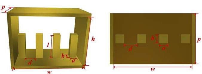
In this paper, a Ka-Band Multi-Corrugated Waveguide(MCW) amplifier using three electron beams is proposed. The SWS(shown in Fig. 1) consists of a rectangular waveguide with four pillars linearly arranged at the bottom of the waveguide. The four pillars are equally separated and three channels are naturally formed. Compared to the DCW, two pillars near the narrow side of the waveguide are added. In this way, two electron channels are added, and at the same time, the coupling impedance can be increased to a certain extent. Using the multi-beam scheme, the beam current is increased and higher output power can be expected.

Figure 1.(a) The perspective for the 3D model of the multi-corrugated waveguide SWS,(b) the top view with dimensional parameters of MCW SWS
A detailed simulation design of the amplifier and cold testing of the interaction structure are carried out. The interaction circuit is fabricated by CNC milling with oxygen-free high conductance copper(OFHCC). The cold test is measured by a 10 MHz to 40 GHz vector network analyzer. The PIC simulation is performed for the circuit with 50 periods SWSs and three beams with 12.9 kV voltage and 67 mA current.
This paper is organized as follows: Section II describes the characteristics of the MCW structure which is simulated by ANSYS Electromagnetics Suit. Section III presents the fabrication details and the cold test results of the MCW structure. In Section IV, the 3D PIC simulation of the MCW TWT is carried out and the performance is compared to DCW TWT. Finally, a simple conclusion is provided.
1 High Frequency Characteristic of the MCW SWS
The MCW is designed based on the Ka-band DCW. Compared to the performance of DCW TWT[17], the MCW TWT is also designed to work in the region of +1st spatial harmonic. The total current of the three beams is 201 mA, which is approximately equal to the current of Ka-band DCW and the beam radius is also set to be 0.25 mm.
According to the analytical model of the corrugated waveguide[18], the pillar length(l), the broadside of the waveguide(w) and the period(p) are the most important factors affecting the dispersion and coupling impedance and are studied here in detail by ANSYS Electromagnetics Suit.
| Symbol | Quantity | Value(mm) |
|---|
| a | The width of the pillar | 0.4 |
| b | The thickness of the pillar | 0.4 |
| d | The distance between pillars | 0.6 |
| l | The length of the pillar | 1.4 |
| h | The high of the waveguide | 2.6 |
| p | The period of the SWS | 2.3 |
| w | The width of the waveguide | 3.6 |
Table 1. Dimension of The MCW SWS
The dispersion and coupling impedance characteristics with the variation of pillar length(l), waveguide width(w), period(p) is shown in Fig. 2. Obviously, the pillar length(l)and the period(p) mainly affect the dispersion and the operating voltage of TWT. The broadside of the waveguide(w)not only affects the dispersion and bandwidth of synchronism, but also significantly affects the coupling impedance. As w increases, the coupling impedance reduces, which will reduce the efficiency of beam-wave interaction.
Figure 2.Dispersion and coupling impedance characteristics with the variation of geometric size (a) the pillar length l, (b) the waveguide width w, (c) the period of MCW p
Combining all the results, the w is set as 3.6 mm, the l is set to be 1.4 mm, and the p is 2.3 mm. Other parameters are also optimized for better bandwidth and interaction impedance. The final chosen parameters are listed in Table 1. And the corresponding dispersion and coupling impedance are shown in Fig. 3, where the beam line is superimposed. Based on this, the beam voltage is determined to be 12.9 kV.
Figure 3.The dispersion curve and coupling impedance of the MCW with dimensions in Table I. note: the beam line of 12.9 kV is superimposed
Compared with the Ka-band DCW[17], the MCW implies quite bandwidth and higher coupling impedance.
2 Microfabrication and Cold Test
In the straight waveguide-type SWSs, the input-output coupler is a very important part, which will affect the performance of the tube. Easy fabricated input-output couplers to minimize reflection are essential for MCW SWS.
In this paper, an input-output coupler is designed. The 20-period MCW SWSs with the input-output coupler is simulated by CST MICROWAVE STUDIO and then fabricated by computer numerical control(CNC) milling. The transmission performance of simulation and cold test are found to be in good consistency.
2.1 Fabrication and Assembly
In the design, the WR28 standard waveguide is adopted to connect the WR28 flanges. As shown in Fig. 4, the interaction circuit is composed of 20-period MCW SWSs and input-output coupler, which includes WR28 waveguide and transition structure. Each transition structure includes 20-period pillars linearly tapered in height from 0.4 mm to 1.4 mm with sloped top. The cross section of the waveguide is also linearly tapered to connect WR28 to MCW.
Figure 4.the 3D model and the assembly sketch of the MCW SWSs
To simplify the fabrication, the model in Fig. 4 is divided into the convex plate with pillars and the upper cover part, which are fabricated respectively. The oxygen-free high conductance copper(OFHCC) is adopted. The fabricated MCW SWS and the microscopic view of the fabricated pillars are shown in Fig. 5. The fabricated tolerance is less than ±5 μm.
Figure 5.Fabricated MCW SWS with input-output coupler
2.2 Simulation and Cold Test
The fabricated MCW in Fig. 5 is cleaned and then measured with a 10MHz to 40 GHz vector network analyzer as shown in Fig. 6.
Figure 6.the photograph of the vector network analyzer and the tested result
In our simulation, the effective conductivity of the fabricated OFHCC is carefully estimated. According to reference[19, 20], the electrical conductivity of metal is primarily affected by surface roughness and skin depth, which can be expressed as:
, is the conductivity with smooth surface, δ is the skin depth, and hs represents the surface roughness and can be described by RMS height of surface.
For OFHCC, is 5.98×10⁷ S/m, the skin depth(δ) is 358 nm at 34 GHz. The surface roughness(hs) of the fabricated OFHCC is estimated to be around 193 nm. Thus, the effective conductivity of the fabricated OFHCC is calculated to be 3.86×10⁷ and used in the simulation.
Fig. 7 shows the comparison between simulation and tested S-parameters of the fabricated MCW SWSs over 30-40 GHz. Obviously, the simulation and test results are very consistent, and in frequency range 32~37 GHz, the simulation and test S11 are less than -15 dB, which meets the engineering requirement.
Figure 7.comparison between simulation and measured S-parameters of the fabricated MCW SWSs
3 Beam-wave interaction simulation
The proposed MCW is simulated by CST PARTICLE STUDIO PIC solver and the beam-wave interaction performance is observed.
In the PIC simulation, the beam voltage and current are set to be 12.9 kV and 0.067 A respectively. A uniform axial focusing magnetic field of 0.4 T is used. The interaction circuit with 50-period SWSs is shown in Fig. 8.
Figure 8.Model of the three-beam MCW circuit in CST PARTICLE STUDIO
The time evolution of the output signal with input signal of 34 GHz and 100 mW input power is shown in Fig. 9. The stable output power is about 132.8 W, indicating a gain of 41.2 dB.
| SWS | Voltage(kV) | Current(mA) | Period number in BWI | Output power(maximum) | Electronic efficiency(maximum) | Gain(maximum) |
|---|
| MCW | 12.9 | 67*3 | 50 | 132.8 W | 5.12% | 41.2 dB |
| DCW | 12 | 200 | 80 | 29 W | 1.2% | 25 dB |
Table 2. Comparison of the DCW[17] and the three-Beam MCW circuit
Figure 9.the variation of input and output signal with time in the frequency of 34 GHz
Fig. 10 shows the spectrum of the output signal, which presents a pure frequency spectrum at the frequency of 34 GHz.
Figure 10.Frequency spectrum of the output signal
Fig. 11 denotes the energy distribution of electron beam. Obviously, there is a strong beam-wave interaction and most of the energy of the electron beam is transferred to the electromagnetic wave.
Figure 11.Energy distribution of electron beam along the transmission direction(z)
Fig. 12 illustrates the output power and gain versus frequency. The gain changes less than 3 dB in the frequency range of 32~37 GHz. The maximum output power is 132.8 W at the frequency of 34 GHz.
Figure 12.the output power and gain versus frequency for the MCW TWT
The electronic efficiency of MCW TWT is plotted in Fig. 13. Within 1 dB bandwidth, it can be seen that the electronic efficiency is higher than 4%.
Figure 13.the electronic efficiency of the MCW TWT in the 29~39 GHz frequency band
The comparison of the performance of the MCW and the DCW[17] is shown in Table 2. In DCW, the beam voltage and the current are 12 kV and 200 mA. Comparatively, the voltage and current of three beams are set to be 12.9 kV and 67 mA.
From Table 2, it can be seen that under similar voltage and total current conditions, the output power, gain and electronic efficiency of MCW are significantly better than DCW. The electronic efficiency of the MCW circuit is even more than four times larger than that of the DCW circuit.
Worth mentioning, in the MCW circuit, 50-period SWSs is used, which is 30 periods less than DCW. This implies to some extent that the beam-wave interaction in the multi-beam MCW is more effective than the single beam DCW circuit. In this way, the MCW circuit has potential application in miniaturization.
4 Conclusion
A multi-beam MCW circuit is proposed to high power and high efficiency TWT amplifier and a three-beam MCW circuit is designed to verify the performance.
The three-beam MCW circuit is designed to work in the frequency range of 32~37 GHz with a low reflection input-output coupler. By CNC milling with OFHCC, the cold test experiment is carried out and S11 less than -15 dB is achieved. The PIC simulation of the MCW shows a significantly better output power, gain and electronic efficiency than DCW. The maximum electronic efficiency and gain are 5.12% and 41.2 dB respectively, larger than 1.2% and 25 dB of DCW.
The proposed multi-beam MCW circuit has important application prospects in high frequency, high power and high efficiency occasions, and exploits a new method for the generation of EM radiation source in point to multipoint transmission millimeter wave wireless system.
References
[1] O QUEVEDO-TERUEL, J MIAO, M MATTSSON et al. Glide-Symmetric Fully Metallic Luneburg Lens for 5G Communications at Ka-Band. IEEE Antennas and Wireless Propagation Letters, 17, 1588-1592(2018).
[2] S SHAKIB, J DUNWORTH, V APARIN et al. mmWave CMOS Power Amplifiers for 5G Cellular Communication. IEEE Communications Magazine, 57, 98-105(2019).
[3] F BOCCARDI, R W H JR, A LOZANO et al. Five Disruptive Technology Directions for 5G. IEEE Communications Magazine, 52, 74-80(2014).
[4] C PAOLONI, R LETIZIA, R ZIMMERMAN et al. W-band TWTs for new generation high capacity wireless networks, 1-2(2016).
[5] A GUPTA, R K JHA. A Survey of 5G Network: Architecture and Emerging Technologies. IEEE Access, 3, 1206-1232(2015).
[6] S S DHILLON, M S VITIELLO, E H LINFIELD et al. The 2017 terahertz science and technology roadmap. Journal of Physics D Applied Physics, 50, 043001(2017).
[7] J S CAYGILL, F DAVIS, S P J HIGSON. Current trends in explosive detection techniques. Talanta, 88, 14-29(2012).
[8] J SWEGLE, E SCHAMILOGLU, J BENFORD. High Power Microwaves, Second Edition. High Power Microwaves, Second Edition Series: Series in Plasma Physics(2007).
[9] Bo CHEN, Qing-Ping ZHAO, Shao-Lun CAI et al. Development of a Ka-band Space TWT, 247-248(2011).
[10] T S RAPPAPORT, S SUN, R MAYZUS et al. Millimeter Wave Mobile Communications for 5G Cellular: It Will Work!. IEEE Access, 1, 335-349(2013).
[11] M MINEO, C PAOLONI. Double-Corrugated Rectangular Waveguide Slow-Wave Structure for Terahertz Vacuum Devices. IEEE Transactions on Electron Devices, 57, 3169-3175(2010).
[12] C PAOLONI, A D CARLO, F BOUAMRANE et al. Design and Realization Aspects of 1-THz Cascade Backward Wave Amplifier Based on Double Corrugated Waveguide. IEEE Transactions on Electron Devices, 60, 1236-1243(2013).
[13] Y SHIN, A BAIG, L R BARNETT et al. System Design Analysis of a 0.22-THz Sheet-Beam Traveling-Wave Tube Amplifier. IEEE Transactions on Electron Devices, 59, 234-240(2012).
[14] J C TUCEK, M A BASTEN, D A GALLAGHER et al. 220 GHz power amplifier development at Northrop Grumman, 553-554(2012).
[15] C C CUTLER. Instability in Hollow and Strip Electron Beams. Journal of Applied Physics, 27, 1028-1029(1956).
[16] H LIANG, Q XUE, C RUAN et al. Integrated Planar Three-Beam Electron Optics System for 220 GHz Folded Waveguide TWT. IEEE Transactions on Electron Devices, PP, 1-7(2017).
[17] C PAOLONI, M MINEO, M HENRY et al. Double Corrugated Waveguide for Ka-Band Traveling Wave Tube. IEEE Transactions on Electron Devices, 62, 3851-3856(2015).
[18] Yu-Lu HU, Xiao-Fang ZHU, C PAOLONI. Study of the dispersion of the double-corrugated waveguide at THz frequencies, 1-2(2016).
[19] S P MORGAN. Effect of Surface Roughness on Eddy Current Losses at Microwave Frequencies. Journal of Applied Physics, 20, 352-362(1949).
[20] M P KIRLEY, J H BOOSKE. Terahertz Conductivity of Copper Surfaces. IEEE Transactions on Terahertz Science and Technology, 5, 1012-1020(2015).