• Laser & Optoelectronics Progress
  • Vol. 56, Issue 16, 163201 (2019)
Zihan Wang1, Baoxu Wang1, Masaru Kamano2, and Weiwei Xu2、*
Author Affiliations
  • 1 State Key Laboratory on Integrated Optoelectronics, College of Electronic Science and Engineering, Jilin University, Changchun, Jilin 130012, China
  • 2 National Institute of Technology, Anan College, Anan, 7740017, Japan
  • show less
    DOI: 10.3788/LOP56.163201 Cite this Article Set citation alerts
    Zihan Wang, Baoxu Wang, Masaru Kamano, Weiwei Xu. Fabrication of Silicon Micro/Nanostructures Based on Laser Interference Ablation[J]. Laser & Optoelectronics Progress, 2019, 56(16): 163201 Copy Citation Text show less
    Mechanism of laser interference ablation on Si. (a) Two-beam interference ablation; (b) HF etching process; (c) final sample
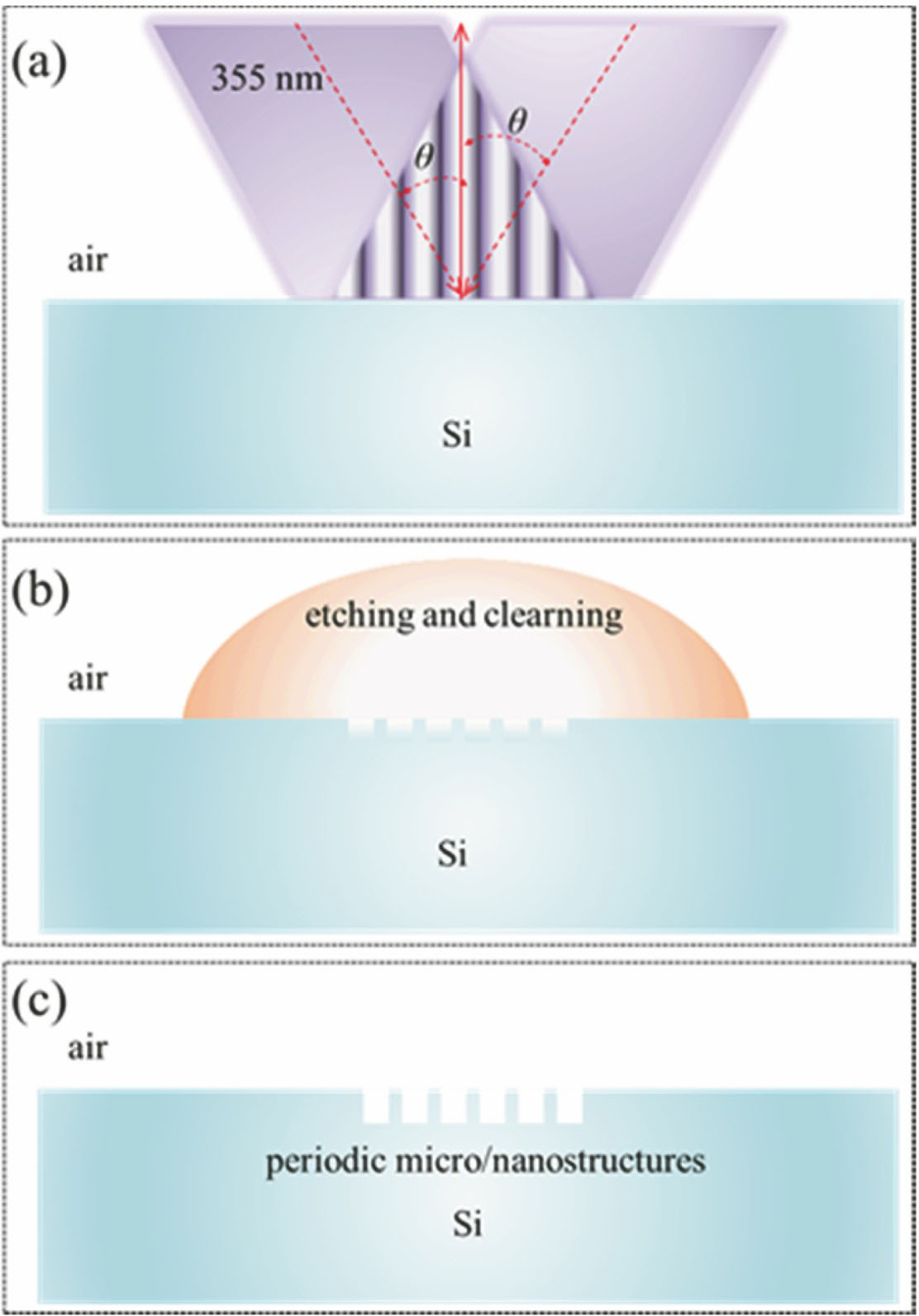
    Fig. 1. Mechanism of laser interference ablation on Si. (a) Two-beam interference ablation; (b) HF etching process; (c) final sample
    Analysis on nanosecond laser interference on Si. (a) Schematic of nanosecond laser interference; (b) maximumlight intensity as a function of period change; (c) surface light intensity distribution of two-beam interference
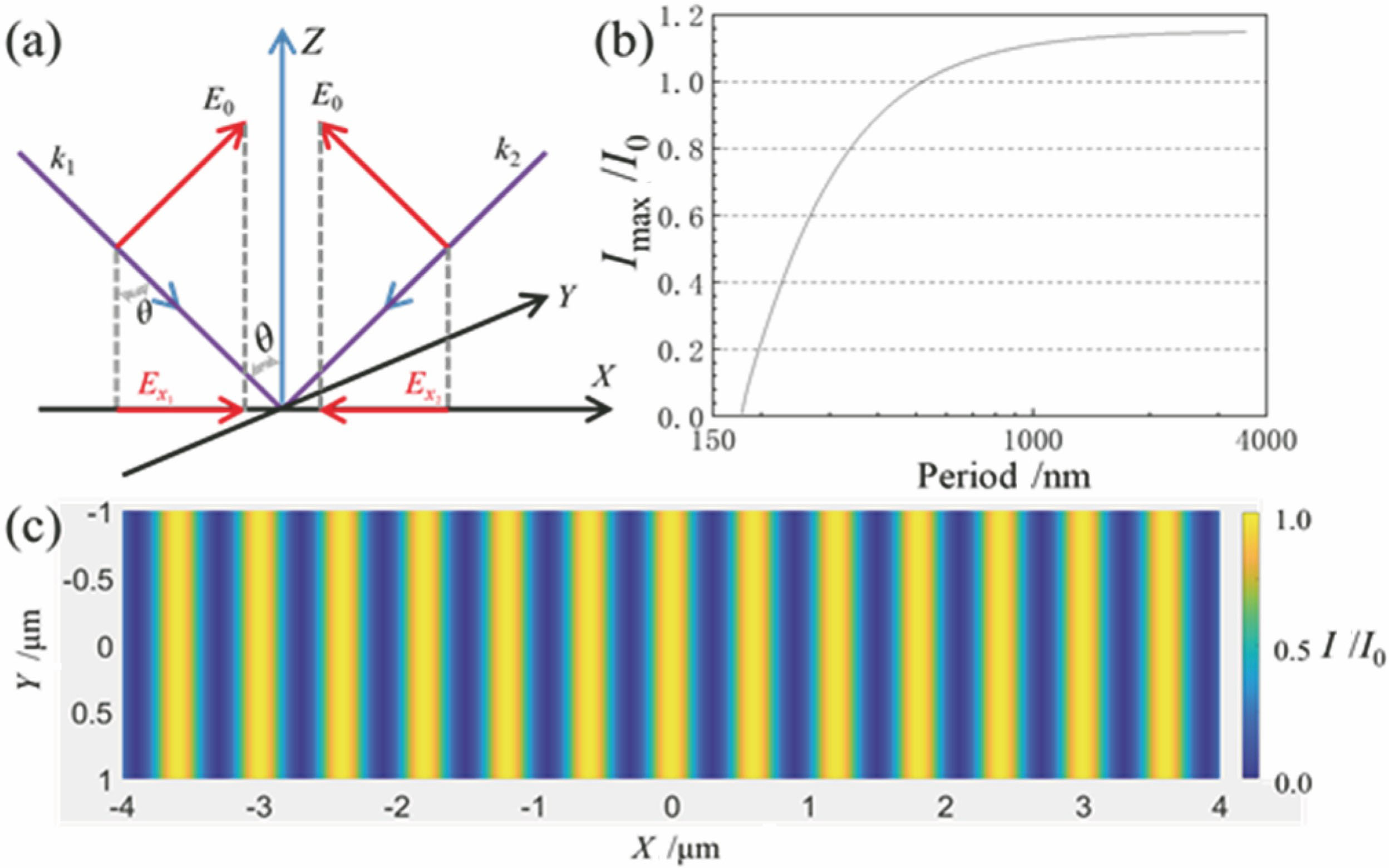
    Fig. 2. Analysis on nanosecond laser interference on Si. (a) Schematic of nanosecond laser interference; (b) maximumlight intensity as a function of period change; (c) surface light intensity distribution of two-beam interference
    Effect of exposure time of laser interference on morphology of periodic micro/nanostructure. (a) Atomic force microscopy (AFM) images at exposure time of 0.5 s; (b) AFM images at exposure time of 1s; (c) AFM images at exposure time of 10 s; (d) AFM images at exposure time of 20 s
    Fig. 3. Effect of exposure time of laser interference on morphology of periodic micro/nanostructure. (a) Atomic force microscopy (AFM) images at exposure time of 0.5 s; (b) AFM images at exposure time of 1s; (c) AFM images at exposure time of 10 s; (d) AFM images at exposure time of 20 s
    Effect of period on structural evolution. (a)-(c) AFM images at exposure time of 1 s, 5 s, and 10 s when period is 1.1 μm; (d) SEM image of Fig. 4(c); (e)-(f) SEM images at exposure time of 1 s and 5 s when period is 0.6 μm; (g) SEM image when period is 300 nm; (h) SEM image of structure ablated by only one beam
    Fig. 4. Effect of period on structural evolution. (a)-(c) AFM images at exposure time of 1 s, 5 s, and 10 s when period is 1.1 μm; (d) SEM image of Fig. 4(c); (e)-(f) SEM images at exposure time of 1 s and 5 s when period is 0.6 μm; (g) SEM image when period is 300 nm; (h) SEM image of structure ablated by only one beam
    Variation in structural depth with exposure time and power. (a) Depth as a function of exposure time; (b) depth as a function of power
    Fig. 5. Variation in structural depth with exposure time and power. (a) Depth as a function of exposure time; (b) depth as a function of power
    FDTD simulation for light intensities propagating in different media. (a) Free space; (b) silicon surface; (c) structured Si surface
    Fig. 6. FDTD simulation for light intensities propagating in different media. (a) Free space; (b) silicon surface; (c) structured Si surface
    Zihan Wang, Baoxu Wang, Masaru Kamano, Weiwei Xu. Fabrication of Silicon Micro/Nanostructures Based on Laser Interference Ablation[J]. Laser & Optoelectronics Progress, 2019, 56(16): 163201
    Download Citation