• Laser & Optoelectronics Progress
  • Vol. 56, Issue 16, 163201 (2019)
Zihan Wang1, Baoxu Wang1, Masaru Kamano2, and Weiwei Xu2、*
Author Affiliations
  • 1 State Key Laboratory on Integrated Optoelectronics, College of Electronic Science and Engineering, Jilin University, Changchun, Jilin 130012, China
  • 2 National Institute of Technology, Anan College, Anan, 7740017, Japan
  • show less
    DOI: 10.3788/LOP56.163201 Cite this Article Set citation alerts
    Zihan Wang, Baoxu Wang, Masaru Kamano, Weiwei Xu. Fabrication of Silicon Micro/Nanostructures Based on Laser Interference Ablation[J]. Laser & Optoelectronics Progress, 2019, 56(16): 163201 Copy Citation Text show less

    Abstract

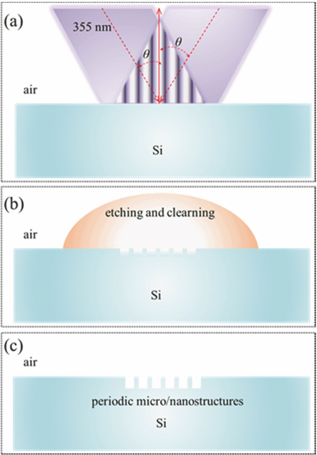
    Based on nanosecond laser two-beam interference ablation assisted with wet-etching method and finite difference time domain (FDTD) simulation, the formation of structures on silicon is studied experimentally and theoretically. The results show that it is possible for the fabrication of structures with period more than 600 nm by a nanosecond laser with wavelength of 355 nm. The structure depth becomes deeper with the increasing of power or exposure time. The maximum depth is equal to the skin depth of laser, about 50 nm. Further, the period splits into half when the exposure time is more than 5 s, which brings a method to obtain a minimum period of 300 nm. The FDTD simulation confirms that the modulation of formed structures to the interference field is the reason for period splitting. The research shows great potential applications for the fabrication of periodic micro/nanostructures, design of maskless processing facilities, and laser-matter interactions.
    Zihan Wang, Baoxu Wang, Masaru Kamano, Weiwei Xu. Fabrication of Silicon Micro/Nanostructures Based on Laser Interference Ablation[J]. Laser & Optoelectronics Progress, 2019, 56(16): 163201
    Download Citation