• Chinese Optics Letters
  • Vol. 20, Issue 3, 031402 (2022)
Lei Han1、2、3, Yuanbin Gao1、2、3, Sheng Hang1、2、3, Chunshuang Chu1、2、3、*, Yonghui Zhang1、2、3, Quan Zheng4, Qing Li4, and Zi-Hui Zhang1、2、3、**
Author Affiliations
  • 1State Key Laboratory of Reliability and Intelligence of Electrical Equipment, Hebei University of Technology, Tianjin 300401, China
  • 2Key Laboratory of Electronic Materials and Devices of Tianjin, School of Electronics and Information Engineering, Hebei University of Technology, Tianjin 300401, China
  • 3Hebei Key Laboratory of Advanced Laser Technology and Equipment, Tianjin 300401, China
  • 4Key Engineering Center of Flat-Panel-Display Glass and Equipment, Shijiazhuang 050035, China
  • show less
    DOI: 10.3788/COL202220.031402 Cite this Article Set citation alerts
    Lei Han, Yuanbin Gao, Sheng Hang, Chunshuang Chu, Yonghui Zhang, Quan Zheng, Qing Li, Zi-Hui Zhang. Impact of p-AlGaN/GaN hole injection layer on GaN-based vertical cavity surface emitting laser diodes [Invited][J]. Chinese Optics Letters, 2022, 20(3): 031402 Copy Citation Text show less
    Schematic diagrams for (a) the conventional InGaN/GaN VCSEL and (b) the InGaN/GaN VCSEL with a p-AlGaN/p-GaN structured p-type hole injection layer, in which polarization induced sheet charges exist at the p-AlGaN/p-GaN interface. The φ1 and φ2 denote the barrier heights at p-EBL/p-GaN and p-EBL/p-AlGaN interfaces, respectively.
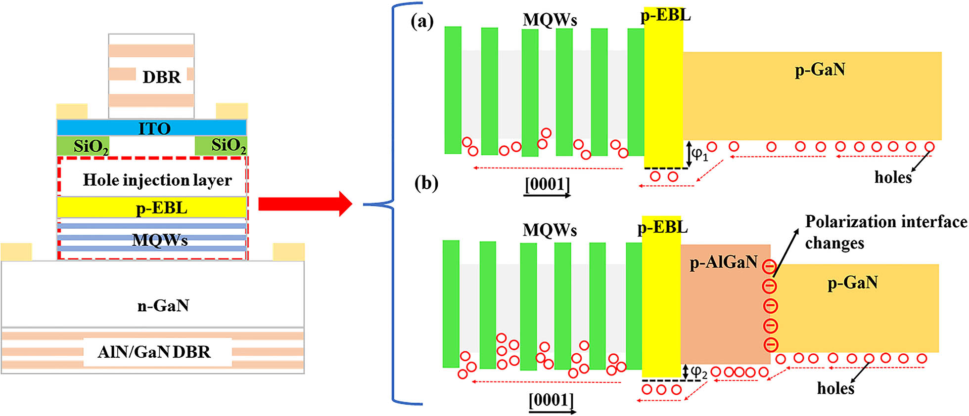
    Fig. 1. Schematic diagrams for (a) the conventional InGaN/GaN VCSEL and (b) the InGaN/GaN VCSEL with a p-AlGaN/p-GaN structured p-type hole injection layer, in which polarization induced sheet charges exist at the p-AlGaN/p-GaN interface. The φ1 and φ2 denote the barrier heights at p-EBL/p-GaN and p-EBL/p-AlGaN interfaces, respectively.
    (a) Hole concentration profiles in the MQWs region, (b) lateral distribution of hole concentration, and (c) hole injection current for VCSELs A and B1 to B3 at 20 mA. (d) Laser power and applied voltage in terms of the injection current for VCSELs A and B1 to B3.
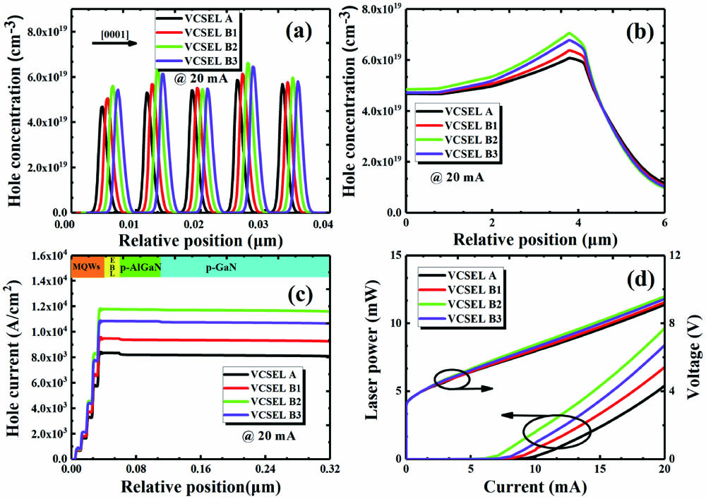
    Fig. 2. (a) Hole concentration profiles in the MQWs region, (b) lateral distribution of hole concentration, and (c) hole injection current for VCSELs A and B1 to B3 at 20 mA. (d) Laser power and applied voltage in terms of the injection current for VCSELs A and B1 to B3.
    (a) Electric field profiles in the p-AlxGa1-xN and p-GaN layers for VCSELs A, B1, B2, and B3, (b) hole concentration profiles in the p-EBL, p-AlxGa1-xN, and p-GaN layers for VCSELs A, B1, B2, and B3, respectively. Data are calculated at the current of 20 mA.
    Fig. 3. (a) Electric field profiles in the p-AlxGa1-xN and p-GaN layers for VCSELs A, B1, B2, and B3, (b) hole concentration profiles in the p-EBL, p-AlxGa1-xN, and p-GaN layers for VCSELs A, B1, B2, and B3, respectively. Data are calculated at the current of 20 mA.
    Valence band profiles in the p-EBL and the p-AlGaN layers for (a) VCSEL A, (b) VCSEL B1, (c) VCSEL B2, and (d) VCSEL B3. Data are calculated at the current of 20 mA.
    Fig. 4. Valence band profiles in the p-EBL and the p-AlGaN layers for (a) VCSEL A, (b) VCSEL B1, (c) VCSEL B2, and (d) VCSEL B3. Data are calculated at the current of 20 mA.
    Calculated small-signal modulation response at the current levels of (a) 1 mA and (b) 20 mA for VCSELs A, B1, B2, and B3. Stimulated radiative recombination rate (Rsti) in the MQWs at the currents of (c) 1 mA and (d) 20 mA for VCSELs A, B1, B2, and B3. Insets of (a) and (b) show 3 dB frequency bandwidth at the currents of 1 mA and 20 mA, respectively.
    Fig. 5. Calculated small-signal modulation response at the current levels of (a) 1 mA and (b) 20 mA for VCSELs A, B1, B2, and B3. Stimulated radiative recombination rate (Rsti) in the MQWs at the currents of (c) 1 mA and (d) 20 mA for VCSELs A, B1, B2, and B3. Insets of (a) and (b) show 3 dB frequency bandwidth at the currents of 1 mA and 20 mA, respectively.
    DevicesVCSEL B1VCSEL B2VCSEL B3
    AlN composition (x)0.020.100.16
    Table 1. Different AlN Compositions of the p-AlxGa1xN Layer for VCSELs B1 to B3
    Lei Han, Yuanbin Gao, Sheng Hang, Chunshuang Chu, Yonghui Zhang, Quan Zheng, Qing Li, Zi-Hui Zhang. Impact of p-AlGaN/GaN hole injection layer on GaN-based vertical cavity surface emitting laser diodes [Invited][J]. Chinese Optics Letters, 2022, 20(3): 031402
    Download Citation