Yu Lu, Lin Kai, Caiyi Chen, Qing Yang, Yizhao Meng, Yi Liu, Yang Cheng, Xun Hou, Feng Chen, "Nanochannels with a 18-nm feature size and ultrahigh aspect ratio on silica through surface assisting material ejection," Adv. Photon. Nexus 1, 026004 (2022)

Search by keywords or author
- Advanced Photonics Nexus
- Vol. 1, Issue 2, 026004 (2022)

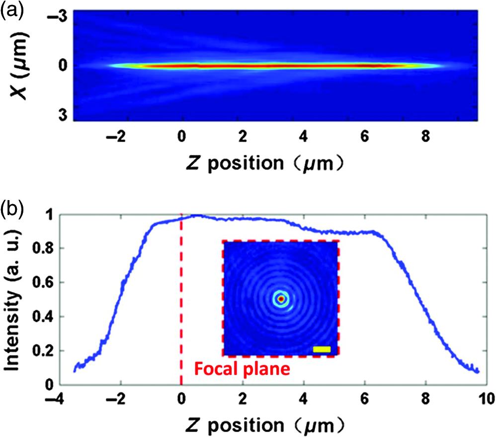
Fig. 1. Energy distribution of the Bessel beam applied for nanochannel fabrication. (a) Longitude section of the Bessel beam energy distribution. (b) The energy accumulation of the core along the axis. (c) Transverse section of the Bessel beam energy distribution. is defined as the focal plane of the objective lens; scale bar: .

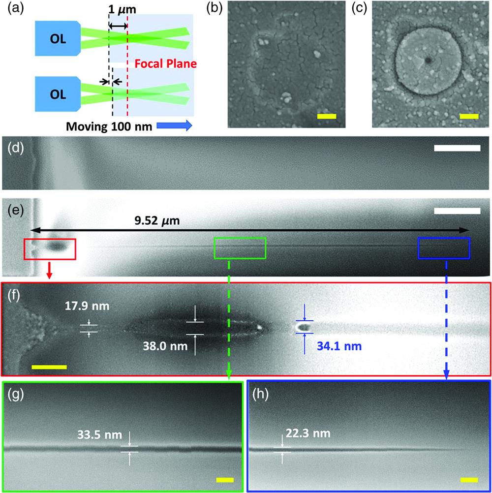
Fig. 2. Single-shot fabrication of nanostructures by a femtosecond Bessel beam with . (a) Experimental step and (b) the SEM image of the superficial nanostructure when the sample surface is put above the focal plane of the objective lens. (c) The SEM image of the superficial nanostructure when the sample surface is put above the focal plane of the objective lens. (d) Inside cross-sectional profile of the nanostructures in (b). (e) Inside cross-sectional profile of the nanostructures in (c). (f) Detailed images of the nanochannel end connecting the surface. (g) Detailed image of the middle part of the nanochannel. (h) Detailed image of the depth end part of the nanochannel. Scale bar: 100 nm for (b), (c) and (f)–(h); for (d) and (e).

Fig. 3. Single-shot fabrication of nanostructures by a femtosecond Bessel beam with pulse energy. (a) The cross-sectional profile of the nanostructures when the sample surface is put above the focal plane of the objective lens. (b) Detailed cross-section image in the vicinity of the surface. (c)–(e) Detailed cross-section images of the interior cavity beneath the sample surface. Scale bar: for (a) and 200 nm for (b)–(d).

Fig. 4. Simulating the temporal evolution of the interaction between the femtosecond Bessel beam and the silica sample. The pulse energy applied in the simulation is . (a)–(c) Temporal evolution of the e-field in the silica sample. To demonstrate the affection of the ionized free electrons to the temporal e-field, the evolution of the electron field is normalized by a temporal normalizer (see Appendix ): (a) 150 fs, (b) 300 fs, and (c) 450 fs. (d) Temporal evolution of the light intensity (left axis and red lines) and the electron density (right axis and blue lines) on the sample surface (solid line) and inside sample (dotted line), respectively. The internal detecting point is beneath the surface. (e) Temporal evolution of the energy deposition speed on the sample surface (solid line) and inside sample (dotted line). The internal detecting position is beneath the surface.

Fig. 5. Energy deposition along the Bessel beam axis depending on the relative position between the femtosecond Bessel beam and the silica sample surface. From the blue and dotted curve to the red and solid curve, the sample surface moved toward the focal plane of the objective lens with a step length of 100 nm.

Set citation alerts for the article
Please enter your email address