Yu Lu, Lin Kai, Caiyi Chen, Qing Yang, Yizhao Meng, Yi Liu, Yang Cheng, Xun Hou, Feng Chen, "Nanochannels with a 18-nm feature size and ultrahigh aspect ratio on silica through surface assisting material ejection," Adv. Photon. Nexus 1, 026004 (2022)
Copy Citation Text
Nanochannel structures with a feature size deeply under the diffraction limit and a high aspect ratio hold huge biomedical significance, which is especially challenging to be realized on hard and brittle materials, such as silica, diamond, and sapphire. By simultaneously depositing the pulse energy on the surface and inside the sample, nanochannels with the smallest feature size of 18 nm (∼1 / 30λ) and more than 200 aspect ratios are achieved inside silica, the mechanism of which can be concluded as the surface assisting material ejection effect. Both the experimental and theoretical results prove that the coaction of the superficial “hot domain” and internal hot domain dominates the generation of the nanochannels, which gives new insights into the laser-material interacting mechanisms and potentially promotes the corresponding application fields.
Nanochannels are widely investigated in many key biomedical and environmental fields, such as nanofluidics,1–3 molecular sieves,4,5 and artificial membranes.6–8 However, it is still a big challenge to realize nanochannels on hard and brittle materials, which show great chemical stabilities and can be applied in many harsh environments. On the surface of some hard brittle materials, such as silicon or other semiconductors, nanochannels with a sub-50-nm size can be realized with lithography techniques, such as deep UV-lithography or electron beam lithography.9–11 Through these lithographic techniques with high precision, superficial directional nanochannels have been widely applied in many biomedical fields, e.g., the DNA stretch.12,13 However, the fabrication of the depth-directional nanochannels, which requires being capable of realizing nanostructures with a large aspect ratio, exceeds the abilities of lithographic techniques.
In the last two decades, femtosecond laser direct writing (FLDW) has become a promising technique in micronanofabrication.14–21 Due to its extremely high peak power and strong nonlinear effect, a femtosecond laser pulse can deposit its energy into nearly any kind of material and achieve effective material removal.18,21 For hard and brittle materials, especially, FLDW has been proved to be capable of fabricating various micronanostructures with 3D complexity on them.22–26 For example, by carefully controlling the pulse energy around the critical intensity, nanopores with a diameter of about 40 nm can be acquired on silica surfaces thorough an evident nonlinear effect by a femtosecond laser, such as multiphoton ionization.22 With the assisting of the localized e-field enhancement effects, complex 2D nanopatterns with a smallest feature size of about 20 nm can be realized on a dielectric film.27 In addition, in the depth direction, nanochannel structures with a sub-50-nm feature size can be realized inside porous glass.23 In this paper, by depositing the pulse energy on the sample surface and deep inside the material with a single-pulse femtosecond Bessel beam,28–30 a material removal effect, named surface assisting material ejection, is induced during the laser–material interaction. Through this effect, nanochannels inside silica with a smallest feature size of 18 nm, which is the smallest reported feature size inside hard and brittle materials, are fabricated. The aspect ratios of these depth-directional nanochannels reach more than 200.
2 Experimental Results
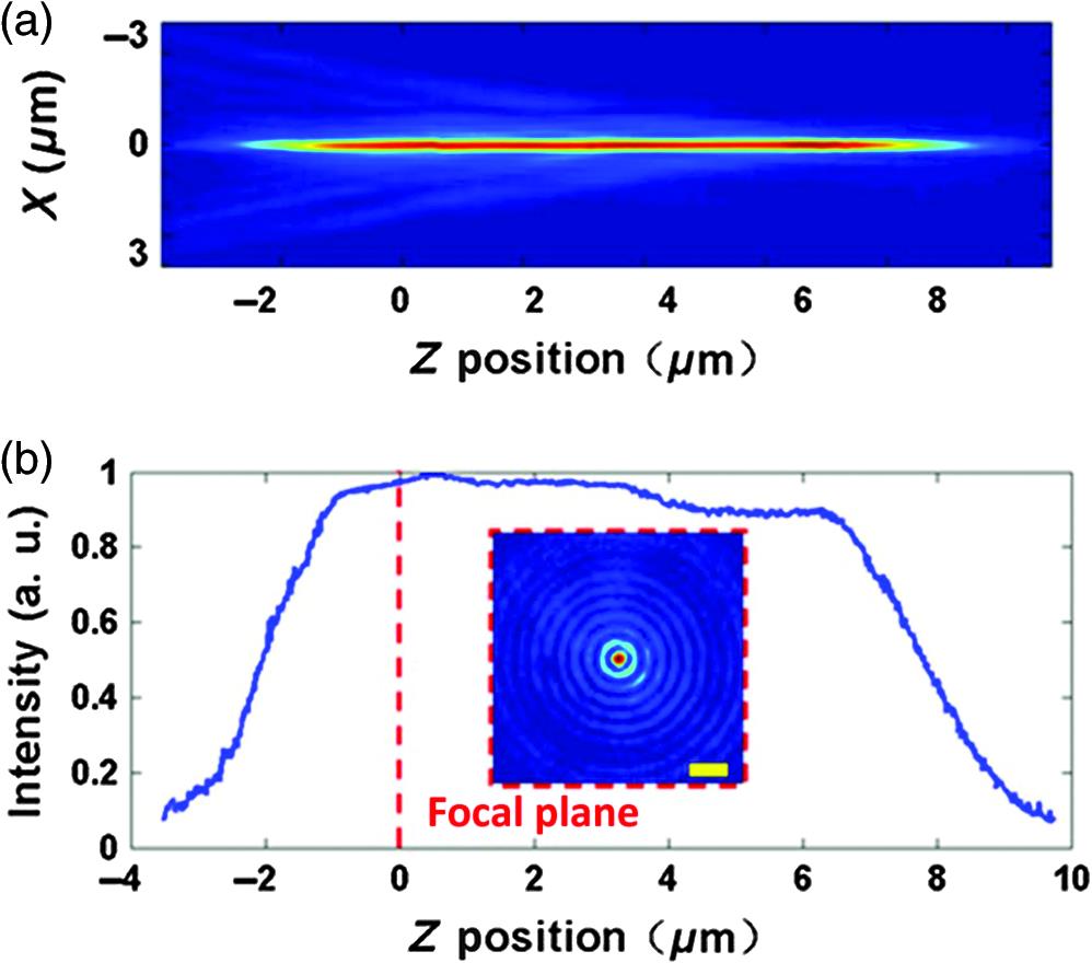
A femtosecond laser with a center wavelength of 1030 nm (FemtoYL-20, YSL photonics) and a pulse width of 300 fs is doubled in frequency into a 515-nm laser. To deposit the laser energy on the sample surface and inside the sample with a single pulse, the femtosecond laser beam with a Gaussian profile is spatially shaped into a Bessel beam through an axicon (AX251-A, Throlabs, 1.0 deg physical angle). The Bessel beam is then compressed onto the silica sample for nanochannel fabrication through a system consisting of a lens with a focal length of 160 mm and an objective lens with the focal lens roughly estimated as 1.6 mm (, 0.8 NA). The silica sample is put on a piezo moving stage in directions with a 10-nm resolution. The intensity distribution of the compressed Bessel beam is observed by a microscope system, which is shown in Fig. 1. As shown in Fig. 1(a), the majority of the energy concentrates in the core of the Bessel beam. The Bessel beam core shows a much higher aspect ratio than the Gaussian beam. The energy accumulation of the core along the axis is shown in Fig. 1(b). From the position of to , the core energy exceeds half of the highest one, indicating that the full-width at half-maximum (FWHM) along the axis is as long as . The energy distribution on the transverse section of the Bessel beam is shown in Fig. 1(c), which is inserted in Fig. 1(b). A group of ring structures surrounds the central core, the diameter of which can be calculated as 374 nm for the FWHM. Correspondingly, the aspect ratio of the Bessel beam core can be calculated as 26.2.
Sign up for Advanced Photonics Nexus TOC. Get the latest issue of Advanced Photonics Nexus delivered right to you!Sign up now
Figure 1.Energy distribution of the Bessel beam applied for nanochannel fabrication. (a) Longitude section of the Bessel beam energy distribution. (b) The energy accumulation of the core along the axis. (c) Transverse section of the Bessel beam energy distribution. is defined as the focal plane of the objective lens; scale bar: .
The focal plane of the objective lens is defined as the plane. The direction along which the compressed Bessel propagates is defined as the axis. In the experiment, the sample stage moves along the plane rapidly and the position of the objective lens and the Bessel beam is fixed. As a result, a single-laser-pulse ablation on the silica sample can be realized. The surface of the sample is first put above the focal plane and is modified in the experiment to modulate the laser–sample interaction. The surface scanning electron microscope (SEM) image of the silica sample ablated by a single femtosecond Bessel pulse with pulse energy is shown in Fig. 2(b). A crater structure with an average diameter of 404 nm can be observed. The silica surface is then moved 100 nm toward the focal plane of the objective lens. As a result, the Bessel beam is “elevated” by 100 nm from the sample relatively, as shown in Fig. 2(a). The superficial nanostructure ablated by the elevated Bessel beam is shown in Fig. 2(c). A crater structure with a diameter of 447 nm exists in which a nanoplate structure with a diameter of 391 nm can be observed. In the center of the nanoplate is a nanohole with a diameter of 27.7 nm. A focused ion beam is used to cut the sample and let the inside cross sections be exposed. An inside cross-section profile of the crater-like images shown in Fig. 2(b) is shown in Fig. 2(d). There is no evident structure beneath the crater. An inside cross-section profile of the crater–plate–hole structures in Fig. 2(c) is shown in Fig. 2(e). Deeply under the sample surface exists a nanochannel as long as . The nanochannel end connecting the surface is shown in Fig. 2(f). From the side view, the nanoplate shape observed in Fig. 2(c) shows a volcano shape. Under the volcano there is a nanocavity structure with the feature size of 38.0 nm. Around the nanocavity, two disconnected parts with feature sizes of 17.9 and 34.1 nm, respectively, can be found. So the nanochannel structure in Figs. 2(e) and 2(f) is not a fully open one. A detailed image of the middle part of the nanochannel structure is shown in Fig. 2(g). The nanochannel shows an almost consistent width in the middle, a typical value of which is measured to be 33.5 nm. The detailed image of the inside end of the nanochannel is shown in Fig. 2(h); the width of the nanochannel at the inside end becomes evidently narrower and finally disappears. Considering the entire length of the nanochannel, the aspect ratio of the nanochannel fabricated in this experiment can be more than 200.
Figure 2.Single-shot fabrication of nanostructures by a femtosecond Bessel beam with . (a) Experimental step and (b) the SEM image of the superficial nanostructure when the sample surface is put above the focal plane of the objective lens. (c) The SEM image of the superficial nanostructure when the sample surface is put above the focal plane of the objective lens. (d) Inside cross-sectional profile of the nanostructures in (b). (e) Inside cross-sectional profile of the nanostructures in (c). (f) Detailed images of the nanochannel end connecting the surface. (g) Detailed image of the middle part of the nanochannel. (h) Detailed image of the depth end part of the nanochannel. Scale bar: 100 nm for (b), (c) and (f)–(h); for (d) and (e).
When improving the pulse energy to , the superficial structures similar to that in Fig. 2(b) can also be discovered with the sample surface moved to above the focal plane of the objective lens. However, as shown in Fig. 3(a), the cross-sectional profile shows evident differences. An interior cavity appears beneath the crater-like nanostructure on the surface. The detailed image of the crater is shown in Fig. 3(b), in which the depth of the crater can be measured as 84.8 nm. The detailed images of the interior cavity are shown in Figs. 3(c)–3(e). The diameters of the interior cavities can be calculated as 140.0, 157.8, and 128.9 nm in Figs. 3(c), 3(d), and 3(e), respectively.
Figure 3.Single-shot fabrication of nanostructures by a femtosecond Bessel beam with pulse energy. (a) The cross-sectional profile of the nanostructures when the sample surface is put above the focal plane of the objective lens. (b) Detailed cross-section image in the vicinity of the surface. (c)–(e) Detailed cross-section images of the interior cavity beneath the sample surface. Scale bar: for (a) and 200 nm for (b)–(d).
It can be seen from Figs. 3(a)–3(e) that two “hot domains” exist. One is on the surface and another one is deep inside the sample. It is easy to conclude that the hot domain on the surface exceeds the boiling temperature (2500 K for silica) and gasifies quickly. The interior hot domain generates the interior cavity inside the sample. Between the two, hot domain is a relatively cool area where no evident void is generated. According to the previous works, this hot domain temperature can be reasonably inferred as more than 4000 K to overcome the confinement from the surrounding cooling materials, including the relatively cool area between the two hot domains, during the cavitation process.31,32 When making a comparison between Figs. 2(d) and 3(a), the conclusion can be gotten that the temperature of the internal hot domain does not exceed the cavitation threshold when using the pulse energy of , as shown in Fig. 2(d). As a result, in Figs. 2(b) and 2(d), only a crater can be observed on the surface and no cavity can be observed beneath. Noting that the pulse energy of is too low to generate an interior cavity by the internal hot domain itself, the generation of the nanochannels with a high aspect ratios in Fig 2(e) can be explained by a mechanism requiring a pulse energy much lower than the cavitation threshold. Through the comparison between Figs. 2(d) and 2(e), this mechanism can be concluded as the surface assisting material ejection, which considers the role that the superficial hot domain played.33 When moving the sample surface toward the high light intensity part of the Bessel beam, as shown in Fig. 2(a), the superficial and internal hot domain approach. With the assistance of the superficial material removal, the internal hot domain can generate the interior cavities without overcoming the surrounding confinement by itself because the gasifying and the material removal of the superficial hot domain will open a window for the material expansion and ejection beneath. The existence of the material ejection can also be proved by the increasing nanoparticle number around the nanoplate–hole structures as well as that around the nanocrater, as shown in Figs. 2(b) and 2(c). Finally, the expansion and ejection of internal material left a nanoplate–hole structure on the surface and the 30-nm diameter nanochannel structure with more than 200 in aspect ratio inside the sample, as shown in Figs. 2(c) and 2(e). In addition, the generation of the two disconnections and the nanocavity in Fig. 2(e) were attributed to the laser–material nonlinear interaction processes, such as self-focusing and filament,34,35 or the material relaxation processes36,37 by previous works. Considering the current experimental results, the self-organization or recast processes may play a more important role than the self-focusing mechanism in the generation of these nanostructures.
3 Theoretical Simulations
To theoretically investigate the generation of the two hot domains and explain the generation of the nanochannels, a simulation of the interaction between the incident femtosecond Bessel beam and the silica sample is made. In the simulations, the ultrafast ionization processes, such as multiphoton ionization and avalanche ionization, which are induced by the femtosecond Bessel beam with peak power, are considered. Correspondingly, the ionized free electrons will also affect the propagation of the femtosecond Bessel beam. The laser energy absorbed by the ionized free electrons will be deposited into the sample, which finally improves the temperature of the sample or leads to material removal (see Appendix). To demonstrate the affection of the ionized free electrons to the e-field, the evolution of the electron field normalized by a temporal normalizer (see Appendix) is shown in Figs. 4(a)–4(c). An almost ideal Bessel beam profile can be found in Fig. 4(a), which means that the normalized e-field strength will maintain the same if the e-field is not affected by the ionized electrons. When it comes to 300 fs, the e-field strength still shows a profile similar to that of a Bessel beam. At 450 fs, however, the e-field profile shows evident deformation. In the vicinity of the core part of the beam, the surrounding e-field is higher than that in the center. The deformation of the e-field profile strength can be attributed to the increase in the electron density. The ionized free electrons generate an electron shield, which will deter the propagation of the e-field to the center part of the Bessel beam. Figure 4(d) checks the temporal evolution of the light intensity and electron density. Different from the e-field strength distribution shown in Figs. 4(a)–4(c), the light intensity in Fig. 4(d) considers the temporal evolution of the incident pulse. Before 200 fs, the internal light intensity increases quickly. However, as the internal electron density begins to increase evidently after 200 fs, the internal light intensity drops rapidly due to the electron shield. After 300 fs, the internal electron density also begins to drop. For the sample surface, the temporal profile of the light intensity is similar to the Gaussian shape, which indicates that the evolution of the surface light intensity is mainly decided by that of the incident laser pulse. The temporal peak of the superficial electron density appears at 450 fs, the value of which is higher than that of the internal peak. The difference in the transient light intensity and electron density between the superficial and internal silica sample also leads to their difference in energy deposition speed, as shown in Fig. 4(e). Before 300 fs, higher energy deposition efficiency happens in the internal domain than on the surface. And then, due to the increase of the electron shield, the energy deposition speed drops quickly in the internal domain. After 400 fs, the energy deposition speed on the surface reaches the peak value. At this time, the energy deposition speed is evidently higher than that beneath. It can be seen from Figs. 4(d) and 4(e) that the energy deposition processes show different mechanisms on the surface and inside the sample. At the detecting point beneath the surface, the light intensity is first higher than that on the surface because when the electron shield is very weak, according to the light intensity distribution along the Bessel beam, as shown in Fig. 1(b), the light at the detecting point is higher than that on the surface. However, the light intensity in the bulk will be strongly affected by the electron shield. As a result, the inside energy deposition drops quickly when the electron density is high. For the sample surface, however, the pulse energy directly incident onto the sample surface from the air, without passing through the internal electron shield in the sample. So it is difficult for the ionized free electrons to affect the superficial e-field. As a result, the energy deposition speed on the surface continues to increase when intense ionization happens, reaching a peak value that is much higher than that beneath.
Figure 4.Simulating the temporal evolution of the interaction between the femtosecond Bessel beam and the silica sample. The pulse energy applied in the simulation is . (a)–(c) Temporal evolution of the e-field in the silica sample. To demonstrate the affection of the ionized free electrons to the temporal e-field, the evolution of the electron field is normalized by a temporal normalizer (see Appendix): (a) 150 fs, (b) 300 fs, and (c) 450 fs. (d) Temporal evolution of the light intensity (left axis and red lines) and the electron density (right axis and blue lines) on the sample surface (solid line) and inside sample (dotted line), respectively. The internal detecting point is beneath the surface. (e) Temporal evolution of the energy deposition speed on the sample surface (solid line) and inside sample (dotted line). The internal detecting position is beneath the surface.
In Fig. 5, by gradually moving the sample surface toward the focal plane of the objective lens in the simulation, the Bessel beam is gradually elevated away from the sample. A series of curves describing the energy deposition distribution along the Bessel beam axis can be acquired. In all curves, both the superficial and the internal hot domains exist. Between the two hot domains, a domain with a relatively lower energy density can be observed. The femtosecond is directly incident onto the sample surface, which is little affected by the ionized free electrons and leads to continuous strong ionization. As a result, the e-field of the area a few hundred nm below the surface suffers a strong shield from the surface electrons, leading to an evident energy deposition drop. With the sample surface approaching the focal plane of the objective lens, the superficial energy deposition changes quickly from to . The peak energy deposition of the “internal” domain remains nearly unchanged at around . For the valley of the “cool domain,” the energy deposition density is first lower than the energy for boiling, which is . Together with moving the sample, the energy depositions in the cool domain also elevate and finally exceed the energy for boiling. In Fig. 5, the existence of the two hot domains is proved from a numerical simulation view. The interaction mechanism between the superficial and the internal hot domain when adjusting their relative distance is also revealed. Their approach will improve the energy deposition of the superficial hot domain and the cool domain between them, which makes the expansion and ejection of the internal material increasingly easier. As a result, when the energy depositions both on the surface and in the cool domain exceed the boiling one, nanochannels can be observed in the hot domain although the energy deposition of it is lower than , which is the threshold value for cavitation. In addition, Fig. 5 also indicates that the modification of the superficial hot domain and the cool domain is sensitive to the relative positions between the Bessel beam and the sample surface, which supports the experimental results in Figs. 2(d) and 2(e).
Figure 5.Energy deposition along the Bessel beam axis depending on the relative position between the femtosecond Bessel beam and the silica sample surface. From the blue and dotted curve to the red and solid curve, the sample surface moved toward the focal plane of the objective lens with a step length of 100 nm.
By depositing the pulse energy on the sample surface and inside the sample with single pulse, nanochannels with the smallest feature size of 18 nm can be acquired, which holds special significance for applications requiring ultranarrow structures, such as ion-gate. The diameter of the channel is 30 nm and the aspect ratio is more than 200. Compared with previous works focusing on nanochannel fabrication, the nanochannels in this work realized the minor averaged diameter reported inside the uniformed hard and brittle material. The aspect ratio of the channel is also comparable with the current works reported. The generation of the nanochannel can be attributed to the surface assisting material ejection effect. Compared with previous works describing the interacting mechanisms between the femtosecond laser and the materials, the surface assisting material ejection takes the role of the sample surface into consideration, through which nanochannels with much smaller feature sizes can be acquired deeply inside the sample with the pulse energy much lower than the traditional cavitation threshold. The inducing of this special surface–interior interaction mechanism relies on depositing the pulse energy on the surface and along the depth direction, which can be realized by a spatially shaping system based on axicons. It is possible for other spatially shaped laser beams with a focal depth much longer than that of the Gaussian beam, such as light needles, to realize similar nanoholes on the sample surface of nanochannels in-depth direction.38–40 The effectiveness of the surface assisting material ejection effect can be proved both experimentally and theoretically. The crater and interior cavity observed when the pulse energy of the femtosecond pulse is high proves the co-existence of the superficial and internal hot domain. Although the internal hot domain cannot lead to the interior cavities when the pulse energy decreases, by making the two hot domains approach each other, the nanochannels referred to can be acquired by inducing the surface assisting material ejection effect. Energy deposition simulation theoretically explains the generating mechanism of this “hot spot” and also reveals their interaction processes. This work can give new insights into the femtosecond laser–material interacting mechanisms and advance many important application fields, such as DNA stretch.
5 Appendix: Simulation Details
In the simulation of this paper, the propagation of the femtosecond Bessel beam can be described by a unidirectional envelope propagation function:41,42
In Eq. (1), is the electric field, which is normalized with a temporal normalizer and . is the pulse energy. is the radius of the incident laser beam compressed by the system described in Sec. 2. The temporal evolution of the incident light laser beam is donated as
In Eq. (2), is the pulse duration. For other parameters in Eq. (1), denotes the group velocity dispersion. denotes the second-order nonlinear effects, such as self-focusing. denotes free electron contribution to the light field, and denotes multiphoton absorption. is the bandwidth of the silica. The temporal evolution of the free electrons is described through the temporal free electron density and the laser intensity , shown as
In Eq. (3), describes the contribution of the multiphoton ionization and tunnel ionization, which can be describe by the Keldysh’s formulation.43 In the simulation, we applied a to describe the contribution of avalanche ionization. describes the lifetime of the free electrons. The energy deposition speed can be expressed as . In Fig. 4(d), the electron is normalized with , which denotes the total density of atoms. All of the parameters in Eqs. (1) and (3) can be found in Refs. 35 and 42.
Yu Lu He received his BS, MS, and PhD degrees in electronic science and technology from Xi’an Jiaotong University in 2013, 2016, and 2021, respectively. He received his PhD degree in biomedical engineering from the City University of Hong Kong in 2021 as collaborating scheme PhD student. His research interests include ultrafast laser fabrication and ultrafast imaging techniques.
Lin Kai received his BS degree in electronic information from Sichuan University. Now, he is a graduate student at Xi’an Jiaotong University. His research interests include ultrafast laser fabrication and ultrafast imaging.
Feng Chen received his BS degree in physics from Sichuan University in 1991 and his PhD in optics from the Chinese Academy of Science in 1997. He is a full professor of electronic engineering at Xi’an Jiaotong University, where he directs the Ultrafast Photonic Laboratory and has serveed as the director of the Shaanxi Key Laboratory of Photonics Technology of Information, a deputy director of the International Joint Research Center for Micro/Nano Manufacturing and Measurement Technologies. He joined the Chinese Academy of Science in 1991, where he was promoted to a full professor in 1999. In 2002, he joined the Xi’an Jiaotong University as a professor and a group leader. His current research interests are femtosecond laser microfabrication, bionic microfabrication, and ultrafast photonics.
Biographies of the other authors are not available.
Yu Lu, Lin Kai, Caiyi Chen, Qing Yang, Yizhao Meng, Yi Liu, Yang Cheng, Xun Hou, Feng Chen, "Nanochannels with a 18-nm feature size and ultrahigh aspect ratio on silica through surface assisting material ejection," Adv. Photon. Nexus 1, 026004 (2022)