• Photonics Research
  • Vol. 3, Issue 6, 317 (2015)
Zeyu Pan1, Harish Subbaraman2, Yi Zou1, Xiaochuan Xu2, Xingyu Zhang1, Cheng Zhang3, Qiaochu Li3, L. Jay Guo3, and Ray T. Chen2、4、*
Author Affiliations
  • 1Microelectronic Research Center, Department of Electrical and Computer Engineering, The University of Texas atAustin, Austin, Texas 78758, USA
  • 2Omega Optics, Inc., 8500 Shoal Creek Blvd, Austin, Texas 78757, USA
  • 3Department of Electrical Engineering and Computer Science, University of Michigan, 1301 Beal Ave, Ann Arbor,Michigan 48109, USA
  • 4Microelectronic Research Center, Department of Electrical and Computer Engineering, The University of Texas at Austin, Austin, Texas 78758, USA
  • show less
    DOI: 10.1364/PRJ.3.000317 Cite this Article Set citation alerts
    Zeyu Pan, Harish Subbaraman, Yi Zou, Xiaochuan Xu, Xingyu Zhang, Cheng Zhang, Qiaochu Li, L. Jay Guo, Ray T. Chen. Quasi-vertical tapers for polymer-waveguide-based interboard optical interconnects[J]. Photonics Research, 2015, 3(6): 317 Copy Citation Text show less
    (a) Schematic of an optical backplane. (b) Schematic of a taper-waveguide system for coupling between standard SMFs and single-mode waveguides. In this diagram, the top cladding is transparent in order to clearly show the system structure, the mode propagating inside the quasi-vertical taper, and the polymer rib waveguide.
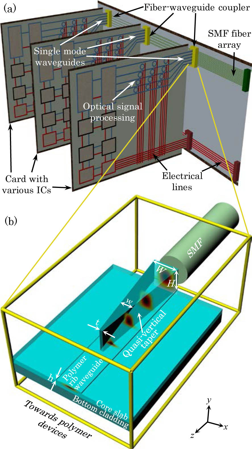
    Fig. 1. (a) Schematic of an optical backplane. (b) Schematic of a taper-waveguide system for coupling between standard SMFs and single-mode waveguides. In this diagram, the top cladding is transparent in order to clearly show the system structure, the mode propagating inside the quasi-vertical taper, and the polymer rib waveguide.
    Mode profile distributions of quasi-TM mode inside the taper at (a) the fiber facet (rib width 8.5 μm, rib height 8 μm), and (b) the device end (rib width 8.5 μm, rib height 0.5 μm). The fundamental (left) and second-order (right) quasi-TM modes (see Visualization 1) for a fixed SU8 rib width of 8.5 μm, and the rib height varying from 14 to 0.5 μm is shown in the supplementary material.
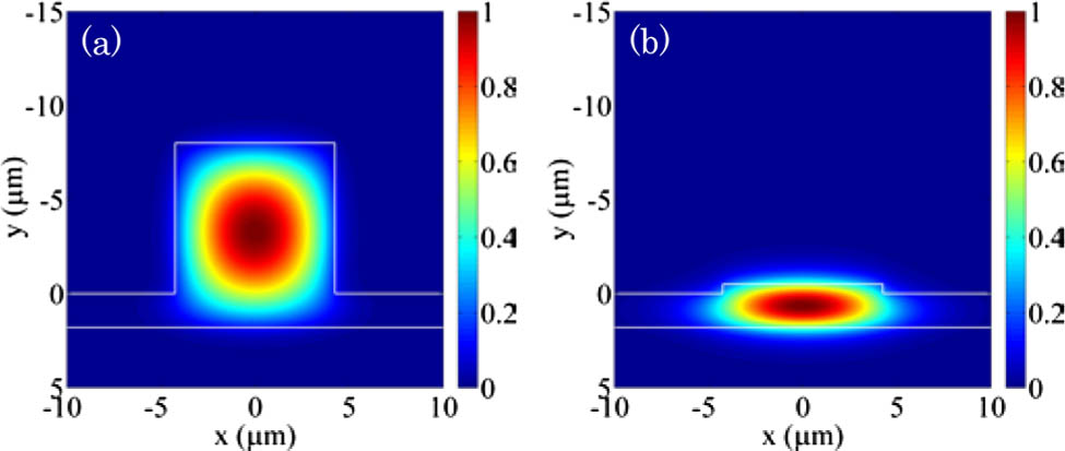
    Fig. 2. Mode profile distributions of quasi-TM mode inside the taper at (a) the fiber facet (rib width 8.5 μm, rib height 8 μm), and (b) the device end (rib width 8.5 μm, rib height 0.5 μm). The fundamental (left) and second-order (right) quasi-TM modes (see Visualization 1) for a fixed SU8 rib width of 8.5 μm, and the rib height varying from 14 to 0.5 μm is shown in the supplementary material.
    Mode profile distributions of quasi-TE mode inside the taper at (a) the fiber facet (rib width 8.5 μm, rib height 8 μm), and (b) the device end (rib width 8.5 μm, rib height 0.5 μm). The fundamental (left) and second-order (right) quasi-TE modes (see Visualization 2) for a fixed SU8 rib width of 8.5 μm and the rib height varying from 14 to 0.5 μm is shown in the supplementary material.
    Fig. 3. Mode profile distributions of quasi-TE mode inside the taper at (a) the fiber facet (rib width 8.5 μm, rib height 8 μm), and (b) the device end (rib width 8.5 μm, rib height 0.5 μm). The fundamental (left) and second-order (right) quasi-TE modes (see Visualization 2) for a fixed SU8 rib width of 8.5 μm and the rib height varying from 14 to 0.5 μm is shown in the supplementary material.
    Coupling efficiency of (a) quasi-TM and (b) quasi-TE mode from a standard SMF into the taper at the fiber facet versus the rib height and rib width of the taper. The white demarcation curve indicates the cut-off region. The bottom left region under the white curve and upper right region above the white curve indicates the single-mode and multimode region, respectively. The intersection point of two white lines indicates the chosen rib height of 8 μm and width of 8.5 μm for the quasi-vertical taper at the fiber facet.
    Fig. 4. Coupling efficiency of (a) quasi-TM and (b) quasi-TE mode from a standard SMF into the taper at the fiber facet versus the rib height and rib width of the taper. The white demarcation curve indicates the cut-off region. The bottom left region under the white curve and upper right region above the white curve indicates the single-mode and multimode region, respectively. The intersection point of two white lines indicates the chosen rib height of 8 μm and width of 8.5 μm for the quasi-vertical taper at the fiber facet.
    (a) Fundamental and (b) second-order quasi-TM modes propagating through the taper into the polymer waveguide. The electric fields are normalized to the maximum electric field of the taper at fiber facet (z=0 μm). The length of the taper is 1.2 mm. Light propagates in the +z direction from left to right. A tip width of 1.8 μm is assumed in this calculation. The cross-sectional electromagnetic field of the fundamental (left) and second-order (right) quasi-TM modes (see Visualization 3) propagating through the quasi-vertical taper at the different locations on the z axis is shown in the supplementary material.
    Fig. 5. (a) Fundamental and (b) second-order quasi-TM modes propagating through the taper into the polymer waveguide. The electric fields are normalized to the maximum electric field of the taper at fiber facet (z=0μm). The length of the taper is 1.2 mm. Light propagates in the +z direction from left to right. A tip width of 1.8 μm is assumed in this calculation. The cross-sectional electromagnetic field of the fundamental (left) and second-order (right) quasi-TM modes (see Visualization 3) propagating through the quasi-vertical taper at the different locations on the z axis is shown in the supplementary material.
    (a) Fundamental and (b) second-order quasi-TE modes propagating through the taper into the polymer waveguide. The electric fields are normalized to the maximum electric field of the taper at fiber facet (z=0 μm). The length of the taper is 1.2 mm. Light propagates in the +z direction from left to right. A tip width of 1.8 μm is assumed in this calculation. The cross-sectional electromagnetic field of the fundamental (left) and second-order (right) quasi-TE modes (see Visualization 4) propagating through the quasi-vertical taper at the different locations on the z axis is shown in the supplementary material.
    Fig. 6. (a) Fundamental and (b) second-order quasi-TE modes propagating through the taper into the polymer waveguide. The electric fields are normalized to the maximum electric field of the taper at fiber facet (z=0μm). The length of the taper is 1.2 mm. Light propagates in the +z direction from left to right. A tip width of 1.8 μm is assumed in this calculation. The cross-sectional electromagnetic field of the fundamental (left) and second-order (right) quasi-TE modes (see Visualization 4) propagating through the quasi-vertical taper at the different locations on the z axis is shown in the supplementary material.
    (a) Calculated optical coupling efficiency of quasi-TM mode from a standard SMF (MFD 10.4 μm) into a polymer waveguide through a quasi-vertical taper versus the misalignment in x (horizontal) and y (vertical) directions. (b) Calculated optical coupling efficiency of quasi-TM mode from a lensed SMF (MFD 2.5 μm) into a polymer waveguide (rib width 8.5 μm and rib height 0.5 μm) without a taper versus the misalignment in x and y direction. (c) Coupling loss of quasi-TM mode in (a) and (b) versus the misalignment in x and y axis.
    Fig. 7. (a) Calculated optical coupling efficiency of quasi-TM mode from a standard SMF (MFD 10.4 μm) into a polymer waveguide through a quasi-vertical taper versus the misalignment in x (horizontal) and y (vertical) directions. (b) Calculated optical coupling efficiency of quasi-TM mode from a lensed SMF (MFD 2.5 μm) into a polymer waveguide (rib width 8.5 μm and rib height 0.5 μm) without a taper versus the misalignment in x and y direction. (c) Coupling loss of quasi-TM mode in (a) and (b) versus the misalignment in x and y axis.
    (a) Calculated optical coupling efficiency of quasi-TE mode from a standard SMF (MFD 10.4 μm) into a polymer waveguide through a quasi-vertical taper versus the misalignment in x (horizontal) and y (vertical) directions. (b) Calculated optical coupling efficiency of quasi-TE mode from a lensed SMF (MFD 2.5 μm) into a polymer waveguide (rib width 8.5 μm and rib height 0.5 μm) without a taper versus the misalignment in x and y direction. (c) Coupling loss of quasi-TE mode in (a) and (b) versus the misalignment in x and y axis.
    Fig. 8. (a) Calculated optical coupling efficiency of quasi-TE mode from a standard SMF (MFD 10.4 μm) into a polymer waveguide through a quasi-vertical taper versus the misalignment in x (horizontal) and y (vertical) directions. (b) Calculated optical coupling efficiency of quasi-TE mode from a lensed SMF (MFD 2.5 μm) into a polymer waveguide (rib width 8.5 μm and rib height 0.5 μm) without a taper versus the misalignment in x and y direction. (c) Coupling loss of quasi-TE mode in (a) and (b) versus the misalignment in x and y axis.
    Fabrication process flow for the quasi-vertical taper. (a) Spin-coat the bottom cladding material (UV15LV) and waveguide slab layer material (SU8 2002) on the substrate. (b) Spin-coat the waveguide rib layer material (SU8 2000.5) and perform the first photolithography step to form the rib core layer of the SU8 polymer waveguide. (c) Spin-coat the top layer material of the quasi-vertical taper (SU8 2007) and perform the second photolithography step to form the triangular region of a taper. (d) Spin-coat the top cladding material (UFC170A).
    Fig. 9. Fabrication process flow for the quasi-vertical taper. (a) Spin-coat the bottom cladding material (UV15LV) and waveguide slab layer material (SU8 2002) on the substrate. (b) Spin-coat the waveguide rib layer material (SU8 2000.5) and perform the first photolithography step to form the rib core layer of the SU8 polymer waveguide. (c) Spin-coat the top layer material of the quasi-vertical taper (SU8 2007) and perform the second photolithography step to form the triangular region of a taper. (d) Spin-coat the top cladding material (UFC170A).
    (a) Top-view SEM image of a fabricated quasi-vertical taper. (b) Cross-section SEM images of a fabricated quasi-vertical taper at fiber facet. Inset in (a) is a zoomed view at the tip.
    Fig. 10. (a) Top-view SEM image of a fabricated quasi-vertical taper. (b) Cross-section SEM images of a fabricated quasi-vertical taper at fiber facet. Inset in (a) is a zoomed view at the tip.
    (a) Schematic and (b) experimental setup to measure the propagation loss of a polymer waveguide. Inset at the top right corner of (b) shows the magnified view of the aligned fibers and the polymer waveguide with quasi-vertical taper.
    Fig. 11. (a) Schematic and (b) experimental setup to measure the propagation loss of a polymer waveguide. Inset at the top right corner of (b) shows the magnified view of the aligned fibers and the polymer waveguide with quasi-vertical taper.
    Measured coupling losses versus the wavelength. The measured coupling losses per taper are 1.79±0.30 and 2.23±0.31 dB for quasi-TM and quasi-TE modes, respectively, for the case of coupling light from a standard SMF (MFD 10.4 μm) to the polymer waveguide through a quasi-vertical taper. The coupling losses per facet are 3.44±0.24 and 3.85±0.24 dB for quasi-TM and quasi-TE modes, respectively, for the case of directly coupling light from a lensed SMF (MFD 2.5 μm) to a polymer waveguide without a taper. Different dashed lines correspond to the simulated coupling losses calculated in Section 2.B. Colors correspond to their respective measured counterpart.
    Fig. 12. Measured coupling losses versus the wavelength. The measured coupling losses per taper are 1.79±0.30 and 2.23±0.31dB for quasi-TM and quasi-TE modes, respectively, for the case of coupling light from a standard SMF (MFD 10.4 μm) to the polymer waveguide through a quasi-vertical taper. The coupling losses per facet are 3.44±0.24 and 3.85±0.24dB for quasi-TM and quasi-TE modes, respectively, for the case of directly coupling light from a lensed SMF (MFD 2.5 μm) to a polymer waveguide without a taper. Different dashed lines correspond to the simulated coupling losses calculated in Section 2.B. Colors correspond to their respective measured counterpart.
    (a) Measured increase in coupling loss of both quasi-TM and quasi-TE modes between the standard SMF (MFD 10.4 μm) and quasi-vertical taper versus horizontal (x axis) and vertical (y axis) misalignment. (b) Measured increase in coupling loss of both quasi-TM and quasi-TE modes between the lensed SMF (MFD 2.5 μm) and polymer waveguide without a taper versus horizontal (x axis) and vertical (y axis) misalignment.
    Fig. 13. (a) Measured increase in coupling loss of both quasi-TM and quasi-TE modes between the standard SMF (MFD 10.4 μm) and quasi-vertical taper versus horizontal (x axis) and vertical (y axis) misalignment. (b) Measured increase in coupling loss of both quasi-TM and quasi-TE modes between the lensed SMF (MFD 2.5 μm) and polymer waveguide without a taper versus horizontal (x axis) and vertical (y axis) misalignment.
    Zeyu Pan, Harish Subbaraman, Yi Zou, Xiaochuan Xu, Xingyu Zhang, Cheng Zhang, Qiaochu Li, L. Jay Guo, Ray T. Chen. Quasi-vertical tapers for polymer-waveguide-based interboard optical interconnects[J]. Photonics Research, 2015, 3(6): 317
    Download Citation