Zeyu Pan, Harish Subbaraman, Yi Zou, Xiaochuan Xu, Xingyu Zhang, Cheng Zhang, Qiaochu Li, L. Jay Guo, Ray T. Chen. Quasi-vertical tapers for polymer-waveguide-based interboard optical interconnects[J]. Photonics Research, 2015, 3(6): 317
Copy Citation Text
A mode transformer based on the quasi-vertical taper is designed to enable high coupling efficiency for interboardlevel optical interconnects involving single-mode polymer waveguides and standard single-mode fibers. A triangular region fabricated above the waveguide is adopted to adiabatically transform the mode from the fiber into the polymer waveguide. The effects of the geometrical parameters of the taper, including width, height, tip width, etc., on the coupling efficiency are numerically investigated. Based on this, a quasi-vertical taper for the polymer rib waveguide system is designed, fabricated, and characterized. Coupling losses of 1.79 _ 0.30 and 2.23 _ 0.31 dB per coupler for the quasi-TM and quasi-TE mode, respectively, are measured across the optical communication C and L bands (1535 to 1610 nm). Low-cost packaging, leading to widespread utilization of polymeric photonic devices, is envisioned for optical interconnect applications.
Polymer-based passive and active photonic devices have been extensively used in various applications, including communication networks [1–12], optical backplanes and interchip interconnects [13–21], sensors [22–32], etc. Low-cost and high-efficiency packaging of these devices is crucial in order to enable an economically viable market. The most prominent methods to couple light into a single-mode polymer waveguide include edge coupling using lensed fiber [1,2,22,33] and surface coupling using grating couplers [34–39]. Although lensed fibers provide acceptable coupling efficiencies, they are more expensive than standard single-mode fibers (SMFs) and are difficult to package due to their limited misalignment tolerance [23,40]. Conventional polymer grating couplers provide limited coupling efficiency in a narrow bandwidth, due to the small refractive index contrast between the polymer materials [38,39]. Some schemes utilize a thin high index coating in order to achieve the required phase matching condition [35–37] and to improve coupling efficiency; still the bandwidth is not large enough to cover both C and L bands. High efficiency, wide bandwidth, and low-cost packaging techniques will tremendously benefit polymer-waveguide-based optical interconnect devices.
In this paper, we design a mode transformer based on a quasi-vertical taper [41–58] to enable high-efficiency coupling between a standard SMF and a single-mode polymer rib waveguide. In this design, a triangular-shape tapered structure is adopted above the waveguide core to transform a fiber mode into a single-mode polymer rib waveguide mode as an optical mode transformer. It comprises of a triangular region with a fixed height, whose width is linearly tapered from the fiber end to a narrow tip at the waveguide end. We experimentally demonstrate a coupling loss of and per coupler for the quasi-TM and quasi-TE mode, respectively, across the C and L bands (1535–1610 nm).
2. DESIGN
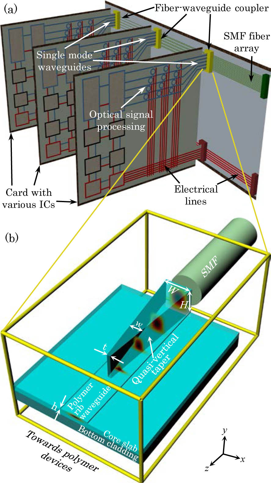
Schematics of an optical backplane for optical interboard interconnects and our designed taper-waveguide system to enable such high-efficiency packaging are shown in Figs. 1(a) and 1(b), respectively. The single-mode polymer waveguide considered in this work consists of a 3.5 μm thick UV15LV ( @ 1.55 μm) bottom cladding; 3 μm thick UFC-170A ( @ 1.55 μm) top cladding; and 2.3 μm thick (1.8 μm slab, rib height, rib width) SU8 ( @ 1.55 μm) core layer. The mode transformer based on a quasi-vertical taper consists of a triangular region with a constant height , whose width is linearly tapered down from at the fiber end to a finite tip width at the waveguide end. We choose these parameters for the triangular taper section based on the coupling efficiency simulations, which will be discussed in Section 2.B. This tapered structure is adopted above the waveguide core to transform the fiber mode into the polymer rib waveguide mode, which works as an optical mode transformer. Because the taper height is higher at the fiber facet than at the single-mode polymer waveguide end, the waveguide mode size in the vertical direction becomes larger at the fiber facets and can better match with the input/output (I/O) fiber mode. Ideally, the tapered tip should be infinitely narrow. However, due to the limited resolution achieved by the photolithography, we fixed the tip width to a finite value. The effect of the tip width on the coupling efficiency will also be discussed in Section 2.B.
Sign up for Photonics Research TOC. Get the latest issue of Photonics Research delivered right to you!Sign up now
Figure 1.(a) Schematic of an optical backplane. (b) Schematic of a taper-waveguide system for coupling between standard SMFs and single-mode waveguides. In this diagram, the top cladding is transparent in order to clearly show the system structure, the mode propagating inside the quasi-vertical taper, and the polymer rib waveguide.
The mode profile distributions of the quasi-TM mode inside the taper at the fiber facet and device end are shown in Figs. 2(a) and 2(b), respectively. The mode profile distributions of the quasi-TE mode at fiber facet [Fig. 3(a)] and device end [Fig. 3(b)] have similar plots shown here for the quasi-TM mode. The polymer waveguide at device end consists of a 1.8 μm thick SU8 core slab and an 8.5 μm wide and 0.5 μm height SU8 core rib. The quasi-vertical taper at the fiber facet consists of a 1.8 μm SU8 core slab and an 8.5 μm wide and 8 μm height SU8 core rib (these values are chosen based on simulation results that will be discussed in Section 2.B). The eigenmodes are calculated using the beam propagation method (RSoft BeamPROP). It can be seen that the mode profile of a polymer waveguide at the device end has a large mismatch with the standard SMF in the vertical direction, while the mode profile of taper at the fiber facet provides a better match with the standard SMF.
Figure 2.Mode profile distributions of quasi-TM mode inside the taper at (a) the fiber facet (rib width 8.5 μm, rib height 8 μm), and (b) the device end (rib width 8.5 μm, rib height 0.5 μm). The fundamental (left) and second-order (right) quasi-TM modes (see Visualization 1) for a fixed SU8 rib width of 8.5 μm, and the rib height varying from 14 to 0.5 μm is shown in the supplementary material.
Figure 3.Mode profile distributions of quasi-TE mode inside the taper at (a) the fiber facet (rib width 8.5 μm, rib height 8 μm), and (b) the device end (rib width 8.5 μm, rib height 0.5 μm). The fundamental (left) and second-order (right) quasi-TE modes (see Visualization 2) for a fixed SU8 rib width of 8.5 μm and the rib height varying from 14 to 0.5 μm is shown in the supplementary material.
We have included two video clips, which show the fundamental (left) and second-order (right) quasi-TM (Visualization 1) and quasi-TE (Visualization 2) modes for a fixed SU8 rib width of 8.5 μm and the rib height varying from 14 to 0.5 μm. When the rib height is smaller than 1.2 μm, the higher-order modes are cut off, and the polymer waveguide becomes a single-mode waveguide. Therefore, the polymer waveguide with a rib height of 0.5 μm can satisfy the single-mode condition. Although the polymer waveguide with a rib height of 8 μm cannot satisfy the single-mode condition, the quasi-vertical taper designed in this paper can filter out these higher-order modes, which will be discussed in Section 2.B.
B. Coupling Efficiency
The fiber coupling efficiency, , can be calculated by a normalized overlap integral between the fiber and waveguide modes [59–61]: where is the function describing the complex amplitude of the SMF, is the function describing the complex amplitude of the waveguide eigenmode, and the ′ symbol represents the complex conjugate.
The coupling efficiencies for the quasi-TM and quasi-TE modes from the standard SMF (e.g., Corning SMF-28) to the single-mode polymer waveguide with different geometries are calculated using Eq. (1). The mode field diameter (MFD) of the standard SMF is 10.4 μm at 1.55 μm wavelength. The coupling efficiency of the quasi-TM and quasi-TE mode from SMF into the quasi-vertical taper at the fiber facet as a function of the rib height and width are plotted in Figs. 4(a) and 4(b), respectively. The white demarcation curve indicates the cut-off region. The upper-right region above the white curve in Fig. 4 indicates the multimode region, while the bottom left region below the white curve indicates the single-mode region. Consequently, we choose the taper rib width at the fiber facet as 8.5 μm and rib height as 8 μm to have a larger coupling efficiency of 84.92% (quasi-TM mode) and 84.84% (quasi-TE mode) with the SMF, and a waveguide rib width of 8.5 μm and rib height as 0.5 μm at the device end to satisfy the single-mode condition.
Figure 4.Coupling efficiency of (a) quasi-TM and (b) quasi-TE mode from a standard SMF into the taper at the fiber facet versus the rib height and rib width of the taper. The white demarcation curve indicates the cut-off region. The bottom left region under the white curve and upper right region above the white curve indicates the single-mode and multimode region, respectively. The intersection point of two white lines indicates the chosen rib height of 8 μm and width of 8.5 μm for the quasi-vertical taper at the fiber facet.
The total coupling efficiency from a standard SMF to a polymer waveguide through a quasi-vertical taper is calculated using the eigenmode expansion method (PhotonDesign FIMMPROP). The total length of the quasi-vertical taper is fixed at 1.2 mm. Considering the limited resolution achieved by the photolithography, the calculated total coupling efficiencies of the quasi-TM mode per coupler are 68.16% (1.66 dB), 73.20% (1.35 dB), 78.56% (1.04 dB), and 83.01% (0.81 dB) for tip widths of 2.0, 1.8, 1.5, and 1.0 μm, respectively. The calculated total coupling efficiencies of the quasi-TE mode per coupler are 71.86% (1.44 dB), 75.43% (1.22 dB), 79.63% (0.98 dB), and 83.33% (0.79 dB) for tip widths of 2.0, 1.8, 1.5, and 1.0 μm, respectively. Therefore, the coupling loss and polarization dependence can be further reduced by using more advanced photolithography instruments to reduce the taper tip width.
The fundamental and higher-order modes propagating through the taper are calculated using the beam propagation method (RSoft BeamPROP). The fundamental and second-order quasi-TM modes propagating though the taper with tip width are shown in Figs. 5(a) and 5(b), respectively. The fundamental [Fig. 6(a)] and second-order [Fig. 6(b)] quasi-TE modes propagating through the taper into the polymer waveguide are similar to Figs. 5(a) and 5(b), respectively. The electric fields are normalized to the maximum electric field of the taper at fiber facet (). As the optical beam propagates through the taper, the mode energy of the fundamental mode is drawn toward the rib and slab region, while the mode energy of the higher-order mode concentrates in the taper region. Thus, the higher-order modes will be filtered by the quasi-vertical taper. Thus, even though the taper supports multiple modes at the fiber facet, it only couples the fundamental mode into the single-mode polymer waveguide. We also include two video clips to show the cross-sectional electromagnetic field of the fundamental (left) and second-order (right) quasi-TM (Visualization 3) and quasi-TE (Visualization 4) modes propagating through the quasi-vertical taper at the different locations on the axis.
Figure 5.(a) Fundamental and (b) second-order quasi-TM modes propagating through the taper into the polymer waveguide. The electric fields are normalized to the maximum electric field of the taper at fiber facet (). The length of the taper is 1.2 mm. Light propagates in the direction from left to right. A tip width of 1.8 μm is assumed in this calculation. The cross-sectional electromagnetic field of the fundamental (left) and second-order (right) quasi-TM modes (see Visualization 3) propagating through the quasi-vertical taper at the different locations on the axis is shown in the supplementary material.
Figure 6.(a) Fundamental and (b) second-order quasi-TE modes propagating through the taper into the polymer waveguide. The electric fields are normalized to the maximum electric field of the taper at fiber facet (). The length of the taper is 1.2 mm. Light propagates in the direction from left to right. A tip width of 1.8 μm is assumed in this calculation. The cross-sectional electromagnetic field of the fundamental (left) and second-order (right) quasi-TE modes (see Visualization 4) propagating through the quasi-vertical taper at the different locations on the axis is shown in the supplementary material.
A larger misalignment tolerance significantly facilitates the device packaging. The misalignment tolerance in the and directions, for the case of direct coupling from a lensed SMF (MFD 2.5 μm) into a polymer waveguide with a rib width of 8.5 μm and a rib height of 0.5 μm [1,33], and from a standard SMF (MFD 10.4 μm) to the quasi-vertical taper is calculated using Eq. (1). Figure 7(a) shows the coupling efficiency of quasi-TM mode versus the (horizontal) and (vertical) misalignments for the case of coupling from the standard SMF (MFD 10.4 μm) into the polymer waveguide through the quasi-vertical taper. Figure 7(b) shows the coupling efficiency of the quasi-TM mode versus the (horizontal) and (vertical) misalignments for the case of direct coupling from the lensed SMF (MFD 2.5 μm) into the polymer waveguide. Figure 7(c) shows the coupling loss of the quasi-TE mode for both cases along the and axes. The corresponding figures for the quasi-TE mode are shown in Figs. 8(a)–8(c), respectively. Compared with using a lensed fiber, utilizing the quasi-vertical taper (tip width 1.8 μm in this calculation), the peak coupling efficiency from a fiber into a polymer waveguide is increased from 49.95% to 73.20% (coupling loss is reduced from 3.02 to 1.35 dB) for the quasi-TM mode, and from 49.67% to 75.43% (coupling loss is reduced from 3.04 to 1.22 dB) for the quasi-TE mode. The 1 dB misalignment tolerance in the vertical direction is increased from 1.25 to 4.33 μm for the quasi-TM mode and from 1.24 to 4.32 μm for the quasi-TE mode, compared with the lensed fiber case. The overall cost of the packaging also can be reduced by using more affordable standard SMFs.
Figure 7.(a) Calculated optical coupling efficiency of quasi-TM mode from a standard SMF (MFD 10.4 μm) into a polymer waveguide through a quasi-vertical taper versus the misalignment in (horizontal) and (vertical) directions. (b) Calculated optical coupling efficiency of quasi-TM mode from a lensed SMF (MFD 2.5 μm) into a polymer waveguide (rib width 8.5 μm and rib height 0.5 μm) without a taper versus the misalignment in and direction. (c) Coupling loss of quasi-TM mode in (a) and (b) versus the misalignment in and axis.
Figure 8.(a) Calculated optical coupling efficiency of quasi-TE mode from a standard SMF (MFD 10.4 μm) into a polymer waveguide through a quasi-vertical taper versus the misalignment in (horizontal) and (vertical) directions. (b) Calculated optical coupling efficiency of quasi-TE mode from a lensed SMF (MFD 2.5 μm) into a polymer waveguide (rib width 8.5 μm and rib height 0.5 μm) without a taper versus the misalignment in and direction. (c) Coupling loss of quasi-TE mode in (a) and (b) versus the misalignment in and axis.
A schematic of the fabrication process is shown in Fig. 9. First, a UV15LV bottom cladding layer is spin-coated on a silicon substrate, then the slab layer (SU8 2002) is spin-coated on top of the bottom cladding layer, as shown in Fig. 9(a). Next, the waveguide rib layer (SU8 2000.5) is spin-coated and patterned using photolithography, as shown in Fig. 9(b). Then, the quasi-vertical taper layer (SU8 2007) is spin-coated, and the taper pattern is defined using another photolithography step, as shown Fig. 9(c). Finally, the top cladding (UFC170A) is spin-coated, as shown in Fig. 9(d).
Figure 9.Fabrication process flow for the quasi-vertical taper. (a) Spin-coat the bottom cladding material (UV15LV) and waveguide slab layer material (SU8 2002) on the substrate. (b) Spin-coat the waveguide rib layer material (SU8 2000.5) and perform the first photolithography step to form the rib core layer of the SU8 polymer waveguide. (c) Spin-coat the top layer material of the quasi-vertical taper (SU8 2007) and perform the second photolithography step to form the triangular region of a taper. (d) Spin-coat the top cladding material (UFC170A).
The top-view and cross-section scanning electron microscope (SEM) images of a fabricated quasi-vertical taper are shown in Fig. 10. Figure 10(a) shows a top view close to the tip, and Fig. 10(b) shows a cross section of the taper at fiber facet. A zoomed image at the tip is shown in the inset of Fig. 10(a). The fabricated tip width is around 1.8 μm, due to the limited resolution of the photolithography process.
Figure 10.(a) Top-view SEM image of a fabricated quasi-vertical taper. (b) Cross-section SEM images of a fabricated quasi-vertical taper at fiber facet. Inset in (a) is a zoomed view at the tip.
The schematic and setup to measure the propagation loss of polymer waveguides is shown in Fig. 11. Light from a broadband infrared continuous-wave ASE source (Thorlabs ASE730) is passed through a polarization controller (OZ Optics FPR-11-11-1550-8/125-P-P-1&2&3-50-3S3S-3-1-), which outputs linearly polarized TM or TE modes with a polarization extinction ratio about 34 dB. A polarization maintaining fiber (OZ Optics PMF-1550-8/125-0.25-L) and a standard SMF (Corning SMF-28), which works as the input and output fiber, respectively, are mounted on an eight-axis positioning stage (Newport PM500-C). The output power is collected by an optical power meter (Newport 2832-C). The inset at the top right corner of Fig. 11(b) shows the magnified view of the aligned fibers and polymer waveguide with quasi-vertical tapers on chip. The measured propagation loss of the polymer waveguide is using the cutback method [56,57].
Figure 11.(a) Schematic and (b) experimental setup to measure the propagation loss of a polymer waveguide. Inset at the top right corner of (b) shows the magnified view of the aligned fibers and the polymer waveguide with quasi-vertical taper.
The coupling loss spectra are measured by an optical spectrum analyzer (OSA, ANDO AQ6317B). The calculated coupling losses spectra from the measured OSA for quasi-TM and quasi-TE polarization are plotted in Fig. 12. The measurement results of the fabricated quasi-vertical taper demonstrate coupling losses of and per coupler for the quasi-TM and quasi-TE modes, respectively, across the C and L bands (1535–1610 nm). For the case of directly coupling light from a lensed SMF to a polymer waveguide without a taper, the measured coupling losses per facet are and for the quasi-TM and quasi-TE modes, respectively. Thus, the quasi-vertical taper can reduce the coupling loss as well as the overall packaging cost. The experimentally measured coupling losses are larger than our calculated values noted in Section 2.B, which is possibly due to the scattering from the fabrication induced roughness. The additional loss for the quasi-TE mode, compared with the quasi-TM mode, is due to the increased scattering from sidewall roughness of the fabricated waveguides.
Figure 12.Measured coupling losses versus the wavelength. The measured coupling losses per taper are and for quasi-TM and quasi-TE modes, respectively, for the case of coupling light from a standard SMF (MFD 10.4 μm) to the polymer waveguide through a quasi-vertical taper. The coupling losses per facet are and for quasi-TM and quasi-TE modes, respectively, for the case of directly coupling light from a lensed SMF (MFD 2.5 μm) to a polymer waveguide without a taper. Different dashed lines correspond to the simulated coupling losses calculated in Section 2.B. Colors correspond to their respective measured counterpart.
The measured increase in coupling loss of both quasi-TM and quasi-TE modes between the standard SMF (MFD 10.4 μm) and quasi-vertical taper for horizontal ( axis) and vertical ( axis) misalignment is shown in Fig. 13(a). The measured increase in coupling loss of both quasi-TM and quasi-TE modes between the lensed SMF (MFD 2.5 μm) and polymer waveguide without a taper for horizontal ( axis) and vertical ( axis) misalignment is shown in Fig. 13(b). The solid curves are the simulation results in Section 2.C. By using the quasi-vertical taper, the measured 1 dB misalignment tolerance in the vertical direction is increased from 1.24 to 4.33 μm, which agrees well with the calculated tolerance in Section 2.C.
Figure 13.(a) Measured increase in coupling loss of both quasi-TM and quasi-TE modes between the standard SMF (MFD 10.4 μm) and quasi-vertical taper versus horizontal ( axis) and vertical ( axis) misalignment. (b) Measured increase in coupling loss of both quasi-TM and quasi-TE modes between the lensed SMF (MFD 2.5 μm) and polymer waveguide without a taper versus horizontal ( axis) and vertical ( axis) misalignment.
A quasi-vertical taper, which is a triangular region on top of the single-mode rib polymer waveguide, is adopted to enable high coupling efficiency from a standard SMF (MFD 10.4 μm) into a single-mode polymer rib waveguide for optical interboard interconnects. Compared with coupling light directly from a lensed SMF (MFD 2.5 μm), the coupling loss is reduced from to for the quasi-TM mode and from to for the quasi-TE mode, across the C and L bands (1535–1610 nm). The 1 dB misalignment tolerance for both quasi-TM and quasi-TE modes is increased from 1.24 to 4.33 μm in the vertical direction. Due to the utilization of standard low cost SMFs for packaging, the overall packaging cost and packaging efforts for the single-mode polymer photonic system can be minimized. Further improvement in the coupling efficiency can be achieved via adopting advanced lithography processes to reduce the taper tip width.
ACKNOWLEDGMENT
Acknowledgment. This work was supported by Air Force Office of Scientific Research (AFOSR) for supporting this work under the Small Business Technology Transfer Research (STTR) program (grant no. FA9550-14-C-0001), monitored by Dr. Gernot Pomrenke.
References
[1] Z. Pan, H. Subbaraman, X. Lin, Q. Li, C. Zhang, T. Ling, L. J. Guo, R. T. Chen. Reconfigurable thermo-optic polymer switch based True-Time-Delay network utilizing imprinting and inkjet printing. Proc. SPIE, 9362, 936214(2014).
[2] Z. Pan, H. Subbaraman, C. Zhang, A. Panday, Q. Li, X. Zhang, Y. Zou, X. Xu, L. J. Guo, R. T. Chen. Reconfigurable thermo-optic polymer switch based true-time-delay network utilizing imprinting and inkjet printing. Terahertz, RF, Millimeter, and Submillimeter-Wave Technology and Applications VIII, 936214(2015).
[4] D. M. Zhang, X. Q. Sun, F. Wang, C. M. Chen. Fast polymer thermo-optic switch with silica under-cladding. 2013 IEEE International Symposium on Next-Generation Electronics (ISNE), 92-94(2013).
[6] X. Wang, B. Howley, M. Y. Chen, Q. Zhou, R. Chen, P. Basile. Polymer-based thermo-optic switch for optical true time delay. Proc. SPIE, 5728, 60-67(2005).
[20] R. T. Chen, L. Wu, F. Li, S. Tang, M. Dubinovsky, J. Qi, C. L. Schow, J. C. Campbell, R. Wickman, B. Picor, M. Hibbs-Brenner, J. Bristow, Y. S. Liu, S. Rattan, C. Noddings. Si CMOS process compatible guided-wave multi-GBit/sec optical clock signal distribution system for Cray T-90 supercomputer. Proceedings of the Fourth International Conference on Massively Parallel Processing Using Optical Interconnections, 10-24(1997).
[35] R. Bruck, R. Hainberger. Efficiency enhancement of grating couplers for single-mode polymer waveguides through high index coatings. Proceedings 14th European Conference on Integrated Optics, 201-204(2008).
[40] Z. Pan, H. Subbaraman, Y. Zou, X. Zhang, C. Zhang, Q. Li, L. J. Guo, R. T. Chen. High optical coupling efficiency quasi-vertical taper for polymer waveguide devices. Proc. SPIE, 9368, 936808(2015).
[44] T. T. Aalto, P. Heimala, S. Yliniemi, M. Kapulainen, M. J. Leppihalme. Fabrication and characterization of waveguide structures on SOI. Proc. SPIE, 4944, 183-194(2003).
[45] I. E. Day, I. Evans, A. Knights, F. Hopper, S. Roberts, J. Johnston, S. Day, J. Luff, H. K. Tsang, M. Asghari. Tapered silicon waveguides for low insertion loss highly-efficient high-speed electronic variable optical attenuators. Optical Fiber Communication Conference, TuM5(2003).
[46] R. J. Bozeat, S. Day, F. Hopper, F. Payne, S. Roberts, M. Asghari. Silicon based waveguides. Silicon Photonics, 269-294(2004).
[50] V. Nguyen, T. Montalbo, C. Manolatou, A. Agarwal, C.-Y. Hong, J. Yasaitis, L. C. Kimerling, J. Michel. Silicon-based highly-efficient fiber-to-waveguide coupler for high index contrast systems. Appl. Phys. Lett., 88, 081112(2006).