
Boyang Wei, Dongmei Liu, Xiuhua Fu, Jing Zhang, Yang Wang, Yu Geng. Study on Film Thickness Uniformity of Magnetron Sputtering System Based on Twin Target[J]. Acta Optica Sinica, 2021, 41(7): 0731001
- Acta Optica Sinica
- Vol. 41, Issue 7, 0731001 (2021)
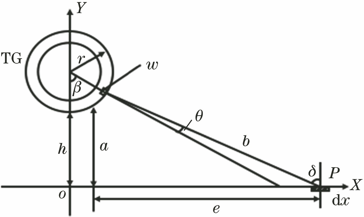
Fig. 1. Schematic of film thickness deposited by twin target magnetron sputtering
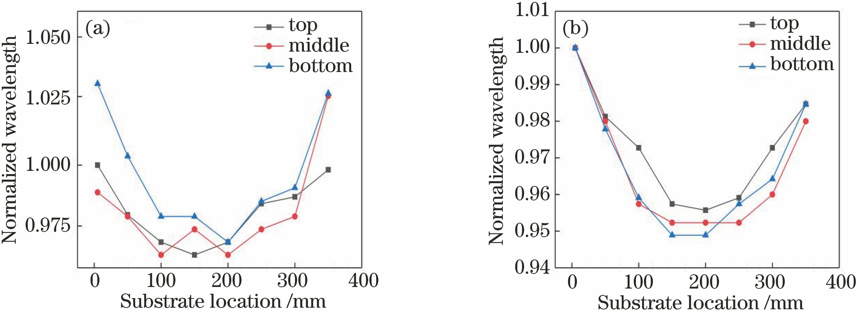
Fig. 2. Horizontal uniformity distribution curves of film thickness of different materials. (a) Si3N4; (b) SiO2
Fig. 3. Corresponding relationship between target magnetic field uniformity and film thickness uniformity under different materials. (a) Si3N4; (b) SiO2
Fig. 4. Influence curves of target base distance of different materials on refractive index. (a) SiO2; (b) Si3N4
Fig. 5. Relationship between plasma density and film thickness of different materials. (a) Si3N4; (b) SiO2
Fig. 6. Uniformity distribution of transverse and longitudinal film thickness
Fig. 8. Longitudinal uniformity curves of film thickness of different materials. (a) Si3N4; (b) SiO2
Fig. 9. Influence curves of film thickness homogeneity under different conditions. (a) Amplitude; (b) phase
Fig. 10. Voltage change curve of target material after loading sinusoidal half wave voltage
Fig. 11. Transverse distribution curves of Si3N4 monolayer film spectrum. (a) Top; (b) middle; (c) bottom
Fig. 12. Transverse distribution curves of SiO2 monolayer film spectrum. (a) Top; (b) middle; (c) bottom
Fig. 13. Spectral distribution curves of hard antireflection film in different directions. (a) Transversal; (b) longitudinal
| |||||||||||||||
Table 1. Transverse uniformity results of two materials

Set citation alerts for the article
Please enter your email address
© Copyright 2018-2021 | Chinese Laser Press. All Rights Reserved 沪ICP备15018463号-20