
Meng-Qiang Cai, Qiang Wang, Cheng-Hou Tu, Yong-Nan Li, Hui-Tian Wang. Dynamically taming focal fields of femtosecond lasers for fabricating microstructures[J]. Chinese Optics Letters, 2022, 20(1): 010502
- Chinese Optics Letters
- Vol. 20, Issue 1, 010502 (2022)
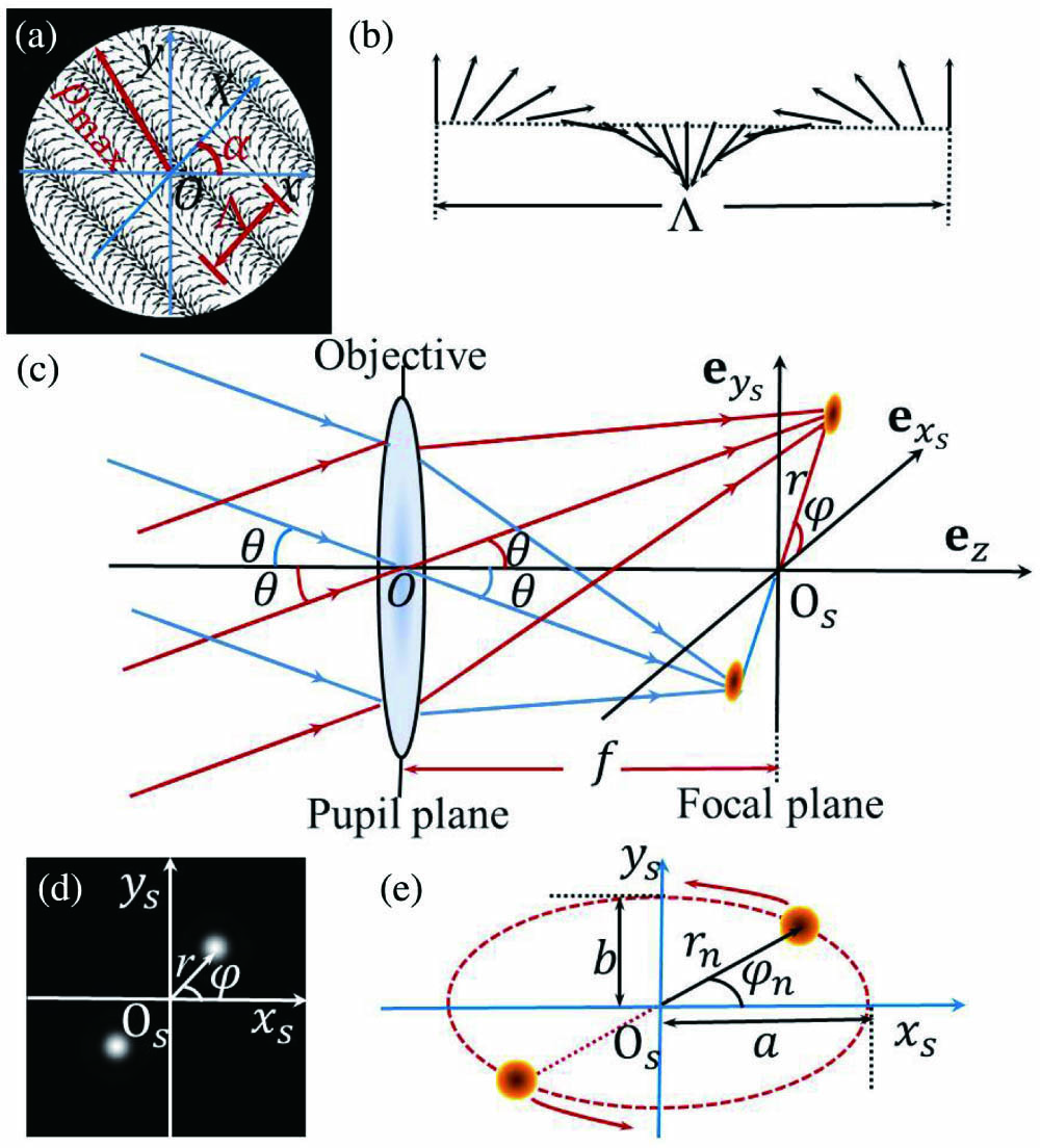
Fig. 1. Realization of a two-spot focal intensity distribution. (a) Schematic diagram of the polarization distribution for the constructed optical field, (b) the polarization variation within one period, (c) the focusing of the constructed optical field with periodic variation in polarization along certain directions in the pupil plane, (d) the corresponding intensity distribution of the focal field, and (e) the formation of an elliptic focal trace.
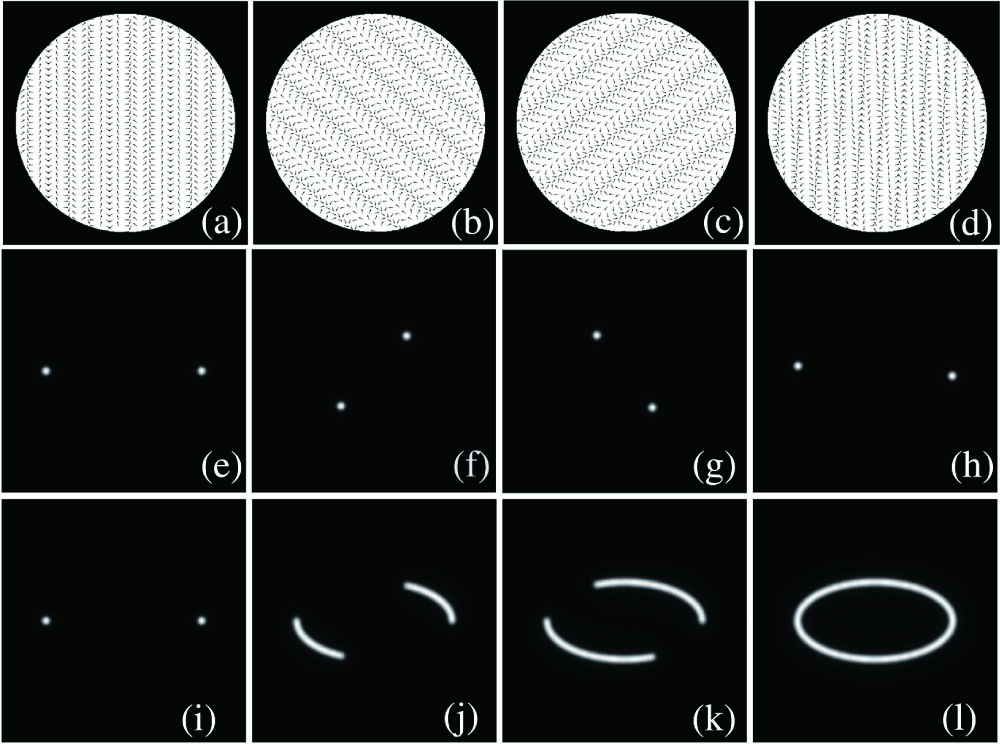
Fig. 2. Schematic diagrams of the elliptic focal trace formation. (a)–(d) are the polarization distributions and the periodic variation of the constructed optical field, and n values are 1, 13, 25, and 37, respectively; (e)–(h) are the corresponding focal field distributions in the focal plane; (i)–(l) are the corresponding produced focal traces when n are 1, 13, 25, and 37, respectively. The size of (e)–(l) is 25 × 25λ2.
Fig. 3. Experiment setup and the corresponding details for the microstructure fabrication. (a) Schematic of experimental setup, (b) and (c) phase distributions for diffractive ±1st-order beams, (d) transmission function of the CGH displayed on the SLM, (e) simulated elliptic focal trace, (f) microscopic imaging of the processed elliptic structure inside the LiNbO3 wafer through the transmitted illumination of white light. The sizes of (e) and (f) are 20 µm × 20 µm.
Fig. 4. Focal spot design by the phase manipulation. (a) A 10 ×10 pixels array with a pixel to be processed, (b) the needed focal spot in the focal plane, (c) the corresponding optical field with periodic variation in phase, and (d) the corresponding intensity distribution of the focal spot.
Fig. 5. Designed and fabricated microstructures. (a) and (d) are, respectively, the binary images with Chinese character “Nan” and irregular quadrilateral grid structure; (b) and (e) are the corresponding simulated patterns of the focal trace; (c) and (f) are the corresponding microscopy images of the fabricated structures. The sizes of (b), (c), (e), and (f) are 20 µm × 20 µm.

Set citation alerts for the article
Please enter your email address
© Copyright 2018-2021 | Chinese Laser Press. All Rights Reserved 沪ICP备15018463号-20