
Meng-Qiang Cai, Qiang Wang, Cheng-Hou Tu, Yong-Nan Li, Hui-Tian Wang. Dynamically taming focal fields of femtosecond lasers for fabricating microstructures[J]. Chinese Optics Letters, 2022, 20(1): 010502
- Chinese Optics Letters
- Vol. 20, Issue 1, 010502 (2022)
Abstract
1. Introduction
Polarization and phase, as the intrinsic nature of light, play important roles in optical field manipulation and various applications. By controlling the polarization state or phase of optical fields, novel optical fields can be obtained, e.g., vector optical field[
As a promising tool for the fabrication of optical devices and microstructures, femtosecond laser processing has been successfully employed to process various materials such as metals, semiconductors, and dielectrics[
In this Letter, we have illustrated the manipulation of optical fields by controlling the polarization or phase periodically varying across the wavefront and then realized certain focal traces by loading dynamical (time-varying) CGH on the SLM. Based on the generated focal traces, we have successfully fabricated microstructures such as an ellipse, an irregular quadrilateral grid structure, and a Chinese character. In terms of the elliptic focal trace, we anticipated that it can be used to cut material along the elliptic trace to fabricate elliptic micro-tubes for microfluidics and to transport particles along the elliptic trace in optical tweezer technology. The benefit of our method is that no motion of samples is needed when fabricating microstructures, and it is more flexible to fabricate an arbitrary micropattern. More importantly, based on our method, any arbitrary freestyle focal trace can be formed. Unlike some methods that use iterative algorithms to generate specific holograms for control focal spots, our method is fast, accurate, and efficient.
Sign up for Chinese Optics Letters TOC. Get the latest issue of Chinese Optics Letters delivered right to you!Sign up now
2. Principle
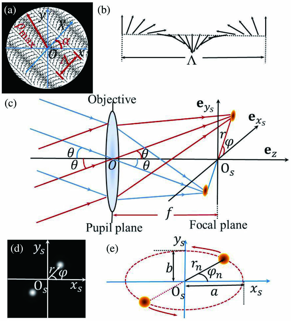
Firstly, we illustrate the realization of a two-spot focal intensity distribution by manipulating the polarization state of an optical field and then the formation of an elliptic focal trace, which is used to fabricate elliptic microstructures. We should note the fact that any freestyle curvilinear trace can be formed based on this method, and herein we just take the formation of an elliptic focal trace as the example. For this purpose, we construct an optical field with the periodic variation in polarization along a certain direction in the pupil plane, as shown in Figs. 1(a) and 1(b), which can be written as
![]()
Figure 1.Realization of a two-spot focal intensity distribution. (a) Schematic diagram of the polarization distribution for the constructed optical field, (b) the polarization variation within one period, (c) the focusing of the constructed optical field with periodic variation in polarization along certain directions in the pupil plane, (d) the corresponding intensity distribution of the focal field, and (e) the formation of an elliptic focal trace.
In Fig. 1(c), we can set the angle between the propagation direction of the beam (or ) and the optical axis ( axis) of the objective to be (or ). As the wave vector is perpendicular to the equiphase surface in free space, we can get ( is the wavelength). According to geometrical optics theory, the optical field (or ) can be focused into one spot, the distance () between the spot and the coordinate origin () in the focal plane is equal to (where is the focal length of the objective), and the azimuthal angle of the spot in the coordinate system is equal to (or ) in the focal plane, as shown by Fig. 1(c), which can be written as .
As the period is far greater than the wavelength , we can make an approximation . Therefore, the relationship between the parameters and can be written as . Based on the Richard–Wolf diffraction integral theory[
To get an elliptic focal trace [see Fig. 1(e)], we just separate the whole ellipse into many discrete points for easy operation (in our case, we use 74 points) and hence simultaneously move the two focal spots point by point; as a result, the two focal spots just need to move 37 positions. The coordinates of a certain spot in the elliptic track can be written as (, ), where , , , and are, respectively, the length of the half-major axis, the length of the half-minor axis, the angle to describe the point located at the elliptic trace, and the integer number of the point in Cartesian coordinates. Therefore, can be achieved through the formula of an elliptic arc length as
In the polar coordinates, the polar coordinates of the corresponding spot can be written as (, ), and and are as follows:
We set and (where ) and substitute them into Eqs. (2)–(4) to get the values of and , which vary with . As shown by Fig. 2, the arrows in Figs. 2(a)–2(d) represent the polarization direction of the incident field, and the manipulation for different polarization states is shown from the left to right, which correspond to , 13, 25, and 37, respectively, while Figs. 2(e)–2(h) show the focal planes of Figs. 2(a)–2(d) after focusing, respectively. It is obvious that the position of the focal point changes as increases. Figs. 2(i)–2(l) show the focal traces when are 1, 13, 25, and 37, respectively. When the value of increases from 1 to 37, the two focal spots move along an ellipse, and finally the elliptic focal trace is formed, as shown in Fig. 2(l). Based on this method, any freestyle curvilinear trace can be formed, and here we just take the elliptic trace for example.
![]()
Figure 2.Schematic diagrams of the elliptic focal trace formation. (a)–(d) are the polarization distributions and the periodic variation of the constructed optical field, and n values are 1, 13, 25, and 37, respectively; (e)–(h) are the corresponding focal field distributions in the focal plane; (i)–(l) are the corresponding produced focal traces when n are 1, 13, 25, and 37, respectively. The size of (e)–(l) is 25 × 25λ2.
3. Experimental Results and Discussion
To fabricate a microstructure, as shown by Fig. 2(l), we firstly generate the optical field expressed in Eq. (1) in experiments and then dynamically vary the parameters of and according to Eqs. (3) and (4) to generate the elliptical focal trace. The experimental setup is shown in Fig. 3(a) (within the dotted line), which is a common path interferometric configuration with the aid of a system composed of a pair of identical lenses (L1 and L2), based on the wavefront reconstruction[
![]()
Figure 3.Experiment setup and the corresponding details for the microstructure fabrication. (a) Schematic of experimental setup, (b) and (c) phase distributions for diffractive ±1st-order beams, (d) transmission function of the CGH displayed on the SLM, (e) simulated elliptic focal trace, (f) microscopic imaging of the processed elliptic structure inside the LiNbO3 wafer through the transmitted illumination of white light. The sizes of (e) and (f) are 20 µm × 20 µm.
, known as the “optical silicon” in the optoelectronic era, has been used as an ideal material for photoelectric chips/integrated devices because of its excellent properties and comprehensive applications in optics and photonics, and hence it is the preferred sample material for our experiment. The optical field is focused beneath the surface of a -cut wafer about 20 µm. Just as mentioned above, when we vary and according to Eq. (4), we can get 37 pairs of focal spots, which finally compose the elliptical focal trace. We know for every point of the focal trace, it corresponds to a pair of and and hence a certain CGH, so we totally need 37 CGHs and then technically combine them to a video to be displayed on the SLM. For every CGH, the displayed time is about 0.02 s, and the whole time spent is about 0.74 s to process an elliptical microstructure. When the energy density of the focal spot is above the threshold inside a wafer, high-order nonlinear absorption allows the energy to be deposited predominantly, which consequently leads to the refractive index modification and induces the morphology change of processed materials[
Secondly, we construct optical fields with linear and periodic variation in phase along a certain direction inspired from Eq. (1), which is as follows:
Based on the former analysis and description, we know the light field expressed by Eq. (6) can be focused into just one circular spot. Similarly, we can also change parameters of and to control the position of the focal spot in the focal plane according to the equations and . With the aid of this fact, we can fabricate arbitrary structures by controlling the focal spot movement.
Supposing the microstructure to be fabricated occupies an area including pixels (where and are the number of columns and rows, respectively), we then create a Cartesian coordinate system with the origin located at the center of the area, as shown in Figs. 4(a) and 4(b). The distance between two adjacent pixels is set to be . Therefore, the coordinates of a given pixel, (, ), can be expressed as (, ), where the subscripts and represent the positional numbers of the column and row, respectively. Because a pixel has an area of , herein we use the coordinates of the lower right vertex of a given pixel to define its coordinates. As a result, the polar coordinates (, ) for the given pixel have the following expression:
![]()
Figure 4.Focal spot design by the phase manipulation. (a) A 10 ×10 pixels array with a pixel to be processed, (b) the needed focal spot in the focal plane, (c) the corresponding optical field with periodic variation in phase, and (d) the corresponding intensity distribution of the focal spot.
According to the equations and , the parameters and of the corresponding incident optical field can be expressed as
To fabricate the above microstructure, what we need to do is just use the coordinate of the pixel to be processed as that of the focal spot in the focal plane and then calculate the corresponding and for the incident light field. Herein, we choose a microstructure with pixels as the example. We choose a pixel whose coordinates are (), as shown by Figs. 4(a) and 4(b), while its polar coordinates are () () according to Eq. (7). Hence, the corresponding parameters and for the incident light field are equal to and , respectively, in the case of according to Eq. (8). The phase variation of the incident optical field is shown in Fig. 4(c), and its focal field corresponds to Fig. 4(d).
Similar to the above example, herein we successfully fabricate a Chinese character and an irregular quadrilateral grid microstructure, which occupy and pixels, respectively. As shown in Figs. 5(a) and 5(d), the binary images (black) of the Chinese character “Nan” and irregular quadrilateral grid structure can be formed based on the pixel array. If each pixel in the array is treated as a single focal point, the combination patterns of these discrete focal points are shown in Figs. 5(b) and 5(e) correspondingly. In order to generate the microstructure pattern in experiment, we need to design the corresponding CGHs to generate the needed focal spots to process some certain pixels. Obviously, according to Eqs. (5), (7), and (8), we can get a series of time-varying CGHs to process all of the pixels. The designed time-varying CGHs are loaded on the SLM to generate phase manipulated optical fields based on the experimental setup shown in Fig. 3(a). However, herein we must block the −1st-order beam to get the optical field expressed by Eq. (6). After focusing, the optical field is irradiated into a wafer with the energy density slightly above the threshold. The fabricated Chinese character of “Nan” and irregular quadrilateral grid microstructure are shown in Figs. 5(c) and 5(f), respectively, and the pixel sizes for them are and , respectively. The line width of the fabricated patterns is about 0.8 µm. Meanwhile, we can see that these microstructures are quite homogeneous and accorded with the simulation results.
![]()
Figure 5.Designed and fabricated microstructures. (a) and (d) are, respectively, the binary images with Chinese character “Nan” and irregular quadrilateral grid structure; (b) and (e) are the corresponding simulated patterns of the focal trace; (c) and (f) are the corresponding microscopy images of the fabricated structures. The sizes of (b), (c), (e), and (f) are 20 µm × 20 µm.
4. Summary
In conclusion, we have designed and generated experimentally optical fields with periodical variation in polarization or phase of the wavefront and realized various focal traces, e.g., an ellipse, a Chinese character “Nan,” and irregular quadrilateral grid structure patterns, which are achieved by loading dynamical CGHs on the SLM. Then, we use these focal traces, which vary dynamically, to interact with wafers and get the corresponding microstructures with a line width about 0.8 µm. Our method provides a movement free dynamic programmable micromachining scheme, and any arbitrary freestyle focal trace can be generated and used to process microstructures, which is stable, cheap, and flexible. Moreover, it is also very promising in many applications, e.g., optical micro devices, optofluidic biochips, and photonic crystals.
References
[1] Q. Zhan. Cylindrical vector beams: from mathematical concepts to applications. Adv. Opt. Photon., 1, 1(2009).
[2] G. J. Gbur. Singular Optics(2016).
[3] Y. Zhang, J. Shen, C. Min, Y. Jin, Y. Jiang, J. Liu, S. Zhu, Y. Sheng, A. V. Zayats, X. Yuan. Nonlinearity-induced multiplexed optical trapping and manipulation with femtosecond vector beams. Nano Lett., 18, 5538(2018).
[4] X. Zhang, G. Rui, J. He, Y. Cui, B. Gu. Nonlinear accelerated orbiting motions of optical trapped particles through two-photon absorption. Opt. Lett., 46, 110(2021).
[5] Y. Kozawa, D. Matsunaga, S. Sato. Superresolution imaging via superoscillation focusing of a radially polarized beam. Optica, 5, 86(2018).
[6] C. Hnatovsky, V. Shvedov, W. Krolikowski, A. Rode. Revealing local field structure of focused ultrashort pulses. Phys. Rev. Lett., 106, 123901(2011).
[7] K. Lou, S. X. Qian, Z. C. Ren, C. Tu, Y. Li, H. T. Wang. Femtosecond laser processing by using patterned vector optical fields. Sci. Rep., 3, 2281(2013).
[8] M. Cai, C. Tu, H. Zhang, S. Qian, K. Lou, Y. Li, H.-T. Wang. Subwavelength multiple focal spots produced by tight focusing the patterned vector optical fields. Opt. Express, 21, 31469(2013).
[9] T. Jiang, S. Gao, Z. N. Tian, H. Z. Zhang, L. G. Niu. Fabrication of diamond ultra-fine structures by femtosecond laser. Chin. Opt. Lett., 18, 101402(2020).
[10] J. Dudutis, J. Pipiras, S. Schwarz, S. Rung, R. Hellmann, G. Račiukaitis, P. Gečys. Laser-fabricated axicons challenging the conventional optics in glass processing applications. Opt. Express, 28, 5715(2020).
[11] K. M. Davis, K. Miura, N. Sugimoto, K. Hirao. Writing waveguides in glass with a femtosecond laser. Opt. Lett., 21, 1729(1996).
[12] B. W. Wu, C. Wang, Z. Luo, J. H. Li, S. Man, K. W. Ding, J. A. Duan. Controllable annulus micro-/nanostructures on copper fabricated by femtosecond laser with spatial doughnut distribution. Chin. Opt. Lett., 18, 013101(2020).
[13] A. Ancona, S. Döring, C. Jauregui, F. Röser, J. Limpert, S. Nolte, A. Tünnermann. Femtosecond and picosecond laser drilling of metals at high repetition rates and average powers. Opt. Lett., 34, 3304(2009).
[14] S. Xu, H. Fan, S.-J. Xu, Z.-Z. Li, Y. Lei, L. Wang, J.-F. Song. High-efficiency fabrication of geometric phase elements by femtosecond-laser direct writing. Nanomaterials, 10, 1737(2020).
[15] M. K. Bhuyan, F. Courvoisier, P.-A. Lacourt, M. Jacquot, L. Furfaro, M. Withford, J. Dudley. High aspect ratio taper-free microchannel fabrication using femtosecond Bessel beams. Opt. Express, 18, 566(2010).
[16] X. Li, M. Li, H. J. Liu. Effective strategy to achieve a metal surface with ultralow reflectivity by femtosecond laser fabrication. Chin. Opt. Lett., 19, 051401(2021).
[17] X. Q. Liu, L. Yu, S. N. Yang, Q.-D. Chen, L. Wang, S. Juodkazis, H.-B. Sun. Optical nanofabrication of concave microlens arrays. Laser Photon. Rev., 13, 1800272(2019).
[18] H. Fan, X.-W. Cao, L. Wang, Z.-Z. Li, Q.-D. Chen, S. Juodkazis, H.-B. Sun. Control of diameter and numerical aperture of microlens by a single ultra-short laser pulse. Opt. Lett., 44, 5149(2019).
[19] X. Jia, T. Jia, L. Ding, P. Xiong, L. Deng, Z. Sun, Z. Wang, J. Qiu, Z. Xu. Complex periodic micro/nanostructures on 6h-sic crystal induced by the interference of three femtosecond laser beams. Opt. Lett., 34, 788(2009).
[20] T. Kondo, S. Matsuo, S. Juodkazis, V. Mizeikis, H. Misawa. Multiphoton fabrication of periodic structures by multibeam interference of femtosecond pulses. Appl. Phys. Lett., 82, 2758(2003).
[21] S. Hasegawa, Y. Hayasaki. Polarization distribution control of parallel femtosecond pulses with spatial light modulators. Opt. Express, 21, 12987(2013).
[22] Y. Jin, O. J. Allegre, W. Perrie, K. Abrams, J. Ouyang, E. Fearon, S. P. Edwardson, G. Dearden. Dynamic modulation of spatially structured polarization fields for real-time control of ultrafast laser-material interactions. Opt. Express, 21, 25333(2013).
[23] R. Drevinskas, J. Zhang, M. Beresna, M. Gecevičius, A. G. Kazanskii, Y. P. Svirko, P. G. Kazansky. Laser material processing with tightly focused cylindrical vector beams. Appl. Phys. Lett., 108, 221107(2016).
[24] M.-Q. Cai, P.-P. Li, D. Feng, Y. Pan, S.-X. Qian, Y. Li, C. Tu, H.-T. Wang. Microstructures fabricated by dynamically controlled femtosecond patterned vector optical fields. Opt. Lett., 41, 1474(2016).
[25] H. Lin, B. Jia, M. Gu. Dynamic generation of Debye diffraction-limited multifocal arrays for direct laser printing nanofabrication. Opt. Lett., 36, 406(2011).
[26] S. Hasegawa, Y. Hayasaki. Holographic femtosecond laser processing with multiplexed phase Fresnel lenses displayed on a liquid crystal spatial light modulator. Opt. Rev., 14, 208(2007).
[27] Y. Hayasaki, T. Sugimoto, A. Takita, N. Nishida. Variable holographic femtosecond laser processing by use of a spatial light modulator. Appl. Phys. Lett., 87, 031101(2005).
[28] J. Ni, C. Wang, C. Zhang, Y. Hu, L. Yang, Z. Lao, B. Xu, J. Li, D. Wu, J. Chu. Three-dimensional chiral microstructures fabricated by structured optical vortices in isotropic material. Light Sci. Appl., 6, e17011(2017).
[29] B. Sun, P. S. Salter, C. Roider, A. Jesacher, J. Strauss, J. Heberle, M. Schmidt, M. J. Booth. Four-dimensional light shaping: manipulating ultrafast spatiotemporal foci in space and time. Light Sci. Appl., 7, 17117(2018).
[30] X.-L. Wang, J. Ding, W.-J. Ni, C.-S. Guo, H.-T. Wang. Generation of arbitrary vector beams with a spatial light modulator and a common path interferometric arrangement. Opt. Lett., 32, 3549(2007).

Set citation alerts for the article
Please enter your email address
© Copyright 2018-2021 | Chinese Laser Press. All Rights Reserved 沪ICP备15018463号-20