Author Affiliations
1School of Electronic and Optical Information, Huazhong University of Science and Technology, Wuhan 430074, China2Wuhan National Laboratory of Optoelectronics, Huazhong University of Science and Technology, Wuhan 430074, China3United Microelectronics Center, Chongqing 400030, Chinashow less
Fig. 1. (Color online) (a) The convergence of electronics and photonics. (b) Design hierarchy of electronic-photonic convergence[2].
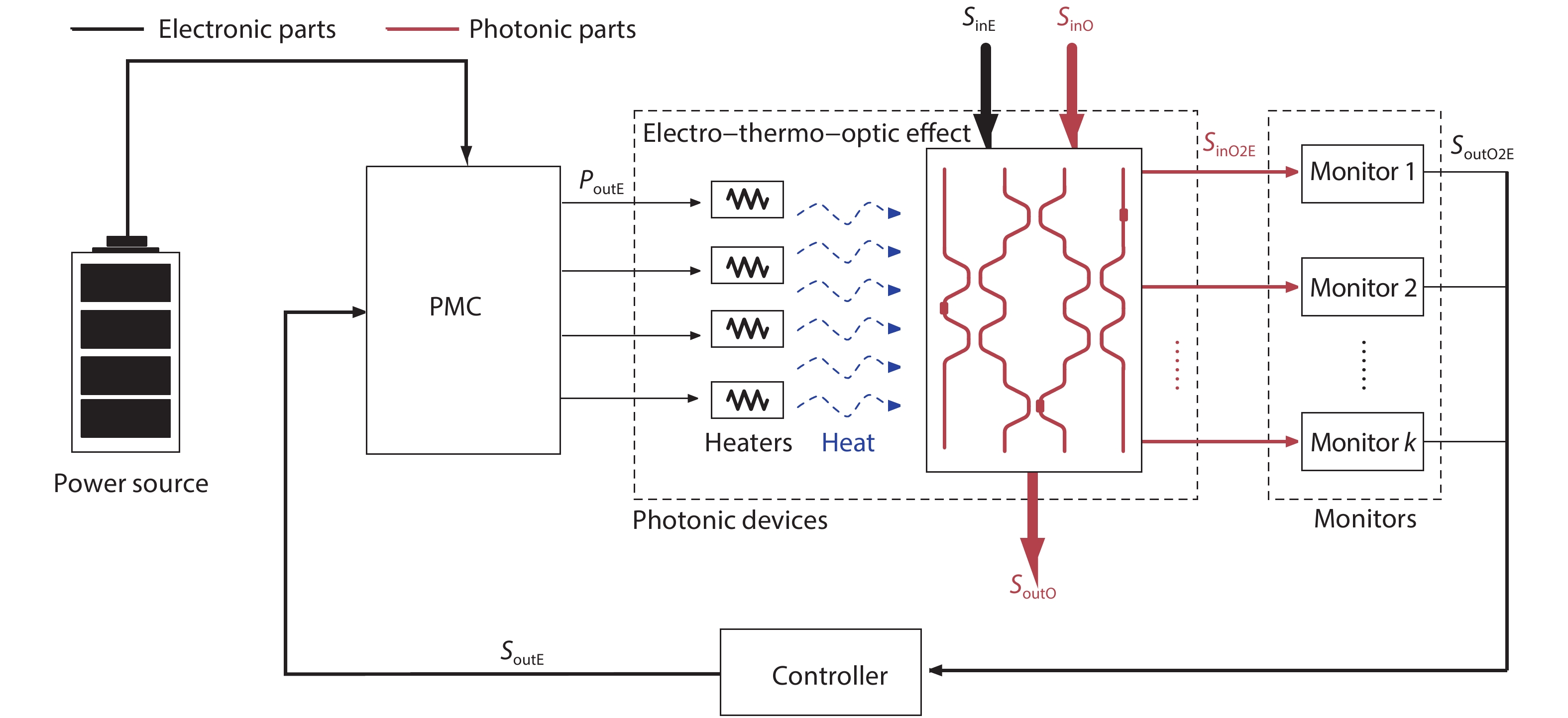
Fig. 2. (Color online) The unified model of a thermo-optic feedback tuning system.
Fig. 3. (Color online) TOPS structures of (a) conventional[6], (b) air-trench[7], (c) multi-bend[8], and (d) multi-pass[9].
Fig. 4. Block diagrams of (a) multiple LDOs and (b) a TDM LDO that drives multiple TOPS.
Fig. 5. Driving the TOPS with (a) DAC and (b) PWM generator.
Fig. 6. (Color online) (a) Cross-section of a photoconductive n-doped silicon waveguide and its integration into a ring resonator to form an IRPH. (b) I–V characteristics of an IRPH with the input laser turned off and on. (c) Calibrated drop-port transmission and photocurrent of a single ring resonator filter relative to its resonance wavelength[35].
Fig. 7. (Color online) Left: Cross-section of the Si core waveguide, with the CLIPP electrode deposited on top of the SiO2 cladding. Right: Longitudinal profile of the Si waveguide showing the CLIPP equivalent circuit in the electrical domain[39].
Fig. 8. (Color online) Operating principle of a pipelined TDM scheme[51].
Fig. 9. (Color online) The general model for thermo-optic feedback wavelength control of a high-order MR filter.
Fig. 10. (Color online) The general model for thermo-optic feedback wavelength locking of an MR modulator.
Fig. 11. Bias control schemes. (a) Output power monitor method. (b) Dithering method. (c) OMA monitor methods.
Fig. 12. The general model for feedback polarization control.
Fig. 13. (Color online) The proof-of-concept prototype in Ref. [69].
Fig. 14. (Color online) A tunable WDM polarization-independent receiver with active polarization control[74].
Fig. 15. The general model for the closed-loop optical phased array.
| Ref. | Undercut | Heater | Pπ (mW) | Size (µm2)
| Bandwidth (kHz) | Loss (dB) | Resistance (Ω) |
|---|
| [7]
| Yes | TiN | 0.4 | 500 × 20 | 0.2 | 0.55 | – | | [8]
| No | Ti | 3.0 | 67 × 28 | 39 | 0.9 | – | | [9]
| No | Metal | 1.7 | 880 × 365 | 53.8 | 6 | – | | [13]
| No | TiN | 2.56 | 109 × 21 | 10.1 | 1.23 | 249.5 | | [14]
| No | TiN | 21.4 | 320 × 2.5 | 62.5 | < 0.4 | 540 | | No | N++Si | 22.8 | 320 × 2.0 | 159 | < 0.4 | 1100 |
|
Table 1. Summary of TOPS designs.
| Ref. | Monitor | Controller | PMC | TOPS | Photonic device | Integration method |
|---|
| [52]
| Photodiode | Lock to Max. | PCB solution | Doping heater | 5-order MR filter | PCB | | [34, 35]
| IRPHs | Lock to Ref. | PCB solution | Doping heater | 4-order MR filter | PCB/Computer | | [54]
| Photodiode | Lock to Min. | PCB solution | Metal heater | 3-order MR filter | PCB | | [55]
| Photodiode | Lock to Max. | PWM | Doping heater | Single MR filter | Monolithic |
|
Table 2. Summary of wavelength control of MR filters.
| Ref. | Monitor | Controller | PMC | TOPS | Photonic device | Integration method |
|---|
| [45]
| Photodiode | Lock to Ref./Average power detection | DAC | Doping heater | Depletion MRM | Wire-bonding | | [56]
| Photodiode | Lock to Ref./Average power detection | PCB solution | Metal heater | Depletion MRM | Off-chip | | [28]
| Photodiode | Lock to Max./OMA maximum | DAC | Metal heater | Depletion MRM | Flip-chip | | [46]
| Photodiode | Lock to Ref./Eye maximum | DAC | c-Si heater | Depletion MRM | Monolithic | | [33]
| Photodiode/Temperature sensor | Lock to Ref./OMA maximum | DAC | Doping heater | Depletion MRM | Monolithic | | [57]
| Photodiode | Lock to Ref./OMA maximum | Power DAC | Metal heater | Depletion MRM | Cu-pillar 3D integration |
|
Table 3. Summary of wavelength locking of a Si MR Modulator.
| Ref. | Monitor | Controller | PMC | TOPS | Photonic device | Integration method |
|---|
| [63]
| Photodiode (power detection) | Lock to Ref | PCB solution | – | LiNbO3 MZM
| Computer | | [64]
| Photodiode (power detection) | Lock to Ref | PCB solution | – | LiNbO3 MZM
| PCB | | [50, 65]
| Photodiode (dithering detection) | Lock to Ref | PCB solution | – | LiNbO3 MZM
| Computer | | [62]
| Photodiode (dithering detection) | Lock to Ref | PCB solution | Metal heater | Silicon MZM | PCB | | [66]
| Photodiode (OMA detection) | Max search | Charge pump | – | LiNbO3 MZM
| Integrated controller | | [67]
| Photodiode OMA + power detection) | Max search and PID control | DAC | – | LiNbO3 MZM
| Integrated controller |
|
Table 4. Summary of bias control schemes.
| Ref. | Monitor | Controller | PMC | TOPS | Photonic device | Integration method |
|---|
| 1. GLD control algorithm.
2. Two-point step size gradient descent-based and two-stage optimization method-based control algorithms.
3. Two-point step size gradient descent-based control algorithms.
| | [69]
| Powermeter | Manual | – | Metal heater | 2DGC/3 dB coupler | – | | [71]
| Photodiode | Min search | PCB solution | Metal heater | Edge coupler/PSR/TOPS/3 dB coupler/PD | Computer | | [70]
| Photodiode | Min search1 | PCB solution | – | 2DGC/GC/OTPS/MMI/PD | Computer | | [73]
| Photodiode | Min search2 | PCB solution | Metal heater | Edge coupler/TOPS/PSR/3 dB asymmetric coupler/PD | Computer | | [74]
| Photodiode | Min search3 | PCB solution | Metal heater | Edge coupler/TOPS/PSR/3 dB coupler/Micro-ring/Crossing/PD | Computer |
|
Table 5. Summary of feedback polarization control schemes.
| Ref. | Monitor | Controller | PMC | TOPS | Photonic device | Integration method |
|---|
| [4]
| Powermeter | – | DAC | Metal heater | Grating coupler optical antenna | Monolithic | | [76]
| IR camera | – | PWM driver | Doping heater | Grating coupler optical antenna | Integrated drivers | | [77]
| Photodetector | – | DAC | Doping heater | Apodized grating antenna | 3D Integrated | | [78]
| IR camera | – | PCB solution | Metal heater | Grating coupler optical antenna | PCB | | [79]
| Photodetector | – | DAC | Doping heater | Grating coupler optical antenna | Monolithic | | [81]
| IR CCD | Gradient-search algorithm | – | Doping heater | Emitter | – | | [82]
| IR CCD | Interference technique | – | – | Grating coupler optical antenna | – | | [83]
| Photodetector | DSGD2 | DAC | – | Emitter | – |
|
Table 6. Summary of the optical phased arrays.

![(Color online) (a) The convergence of electronics and photonics. (b) Design hierarchy of electronic-photonic convergence[2].](/richHtml/jos/2021/42/2/023104/img_1.jpg)