
Min Tan, Kaixuan Ye, Da Ming, Yuhang Wang, Zhicheng Wang, Li Jin, Junbo Feng. Towards electronic-photonic-converged thermo-optic feedback tuning[J]. Journal of Semiconductors, 2021, 42(2): 023104
- Journal of Semiconductors
- Vol. 42, Issue 2, 023104 (2021)
Abstract
1. Introduction
Due to both physical and economic limits, Moore’s law is approaching its end. Meanwhile, new applications are emerging rapidly, raising energy efficiency, capacity, and data rate challenges. Many post-Moore's directions are proposed to address the above challenges. Integrated photonics is among the most promising ones, as it offers the benefits of high data rate, low transmission loss, wide spectrum range, etc. Integrated photonics, especially silicon photonics, has made tremendous progress in the past few years. By leveraging the microelectronics fabrication platform, large-scale device fabrication and integration is made possible with silicon photonics.
Nevertheless, integrated photonics lacks practical photonic registers and flexible control and needs to be combined with electronics for any practical purpose. Integrated photonic devices suffer from many uncertainties, such as fabrication errors, supply voltage changes, and temperature variations. In many situations, these uncertainties prevent the devices from reliable operations.
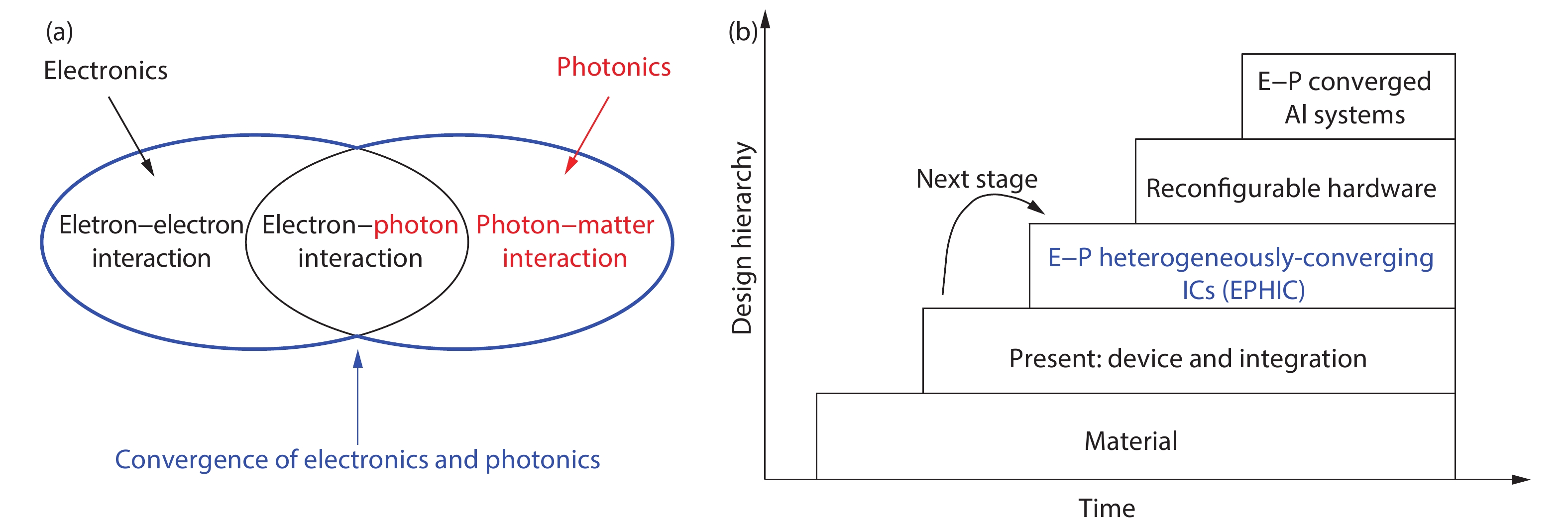
Feedback tuning is an effective approach to maintain reliable operations of these photonic devices. For example, the resonant wavelength of a micro-ring is strongly affected by the process and temperature variations, and a feedback stabilization loop is required to fix the wavelength. For dynamic operations, a feedback mechanism is also required to ensure that the photonic devices are operating at the desired operating point. For example, we monitor the status of optical switches and set it to the expected operating state. Thus, for both stability and dynamic operations considerations, feedback photonic parameter tuning is required. Many tuning mechanisms have been proposed in the literature. The thermo-optic effect is among the most frequently used ones due to the advantages of high efficiency and low loss. Up to now, most thermo-optic feedback tuning solutions use PCB-level or benchtop solutions. These conventional solutions are no longer suitable for large-scale integration, and the convergence of electronics and photonics is an irresistible trend[
![]()
Figure 1.(Color online) (a) The convergence of electronics and photonics. (b) Design hierarchy of electronic-photonic convergence[
The remainder of this paper is organized as follows. Section 2 proposes a unified model for thermo-optic feedback tuning and discusses its design challenges. Section 3 focuses on each building blocks. Section 4 reviews the state-of-the-art designs. Section 5 points out future trends. Section 6 concludes this paper.
2. Unified model and challenges
Fig. 2 shows the unified model for the design and analysis of a thermo-optic feedback tuning system. The photonic part consists of one or multiple devices, possibly with multiple photonic inputs and multiple photonic outputs. Furthermore, it may have multiple open-loop electronic input signals and multiple closed-loop electronic input signals. The monitors obtain the status information of the photonic devices, e.g., the wavelength of a micro-ring resonator, beamforming direction of an optical phased array (OPA), etc. After processing the monitoring information, the controller passes the processed signal to a power management circuit (PMC) for thermo-optical tuning.
![]()
Figure 2.(Color online) The unified model of a thermo-optic feedback tuning system.
There are multiple challenges for thermo-optic feedback tuning. From the microelectronics industry's experiences, to cope with the increasing design complexity, compact device modeling and design automation tools need to be developed. Also, we need to develop cost-efficient, reliable, and efficient monitoring techniques. Furthermore, a low-power and compact controller is required. Compared with conventional power converters for electronics, thermo-optic tuning has a different power and voltage ranges, loading conditions, and bandwidth requirements and brings new design challenges and opportunities. Many applications, such as optical phased array and optical switches, requires a large number of heaters, and scalability is the key challenge. For the thermo-optic phase shifter (TOPS), it is quite challenging to reduce its power consumption while achieving a wide bandwidth. TOPS has been used in many applications, such as the wavelength tuning of micro-ring modulators, bias tuning of Mach–Zehnder modulators, polarization control, optical neural network (ONN)[
3. Building blocks
The performance of thermo-optic feedback tuning critically depends on that of its building blocks. So far, most building blocks use PCB or benchtop solutions and very few of them adopted integrated solutions. In this section, we discuss the research progress of each building block.
3.1. Thermo-optic phase shifting
A typical thermo-optic phase shifter (TOPS) consists of a waveguide and a heater (a purely resistive load). The heat generated by the heater diffuses to the waveguide and changes its refractive index. Putting the heater closer to the waveguide reduces the diffusing time but increases the optical loss. Vice versa, putting the heater farther from the waveguide reduces the optical loss but results in more power consumption and reduced bandwidth. The performance of a TOPS depends on its material and structure. There are tradeoffs in TOPS designs, and different techniques have been proposed to optimize the TOPS performances.
The conventional structure is shown in Fig. 3(a)[
![]()
Figure 3.(Color online) TOPS structures of (a) conventional[
The thermo-optic performance also depends on the materials of the waveguide and the heater. SOI waveguide has high absorption in some spectral bands, e.g., 532–900 nm wavelength window[
3.2. Power management circuit (PMC)
Most TOPS designs apply PCB or benchtop power supplies. These solutions are not practical for large-scale integrated systems, and an integrated power supply is the key to achieve a compact footprint. Low-dropout (LDO) regulator is the preferred power supply, especially for supplying many heaters, as it can be fully integrated and has a compact chip area and accurate output voltage with a small ripple. So far, power management circuit (PMC) specific to thermal-tuning is still in its early development stage. Different from conventional LDO applications, thermo-optical tuning has different requirements. To support a large temperature tuning range, a large output range is required. To reduce the unwanted heat generation, a high efficiency is required. For fast thermo-optic tuning, a wide bandwidth is required. To enable high scalability, a small chip area is required. The required power for each TOPS is in the range of tens of mWs. Consequently, the power stage of the LDO is much smaller than conventional applications. To reduce the chip area, Ref. [22] proposed to share the controller between different channels with the time-division multiplexing (TDM) scheme. Fig. 4 shows the comparison between the conventional way and the TDM LDO to drive multiple TOPSs. As each TOPS's required tuning power is relatively small, the controller occupies a large percent of the total chip area. Sharing the controller saves the total chip area and improves system scalability.
![]()
Figure 4.Block diagrams of (a) multiple LDOs and (b) a TDM LDO that drives multiple TOPS.
There are two popular methods to control the LDO: the output of a DAC[
![]()
Figure 5.Driving the TOPS with (a) DAC and (b) PWM generator.
3.3. Monitor
The monitor senses the operating state of the photonic devices. Various techniques have been proposed in the literature: (1) on-chip photodetectors (PDs) to monitor the light intensity at the output ports[
On-chip PDs are the most commonly used monitoring method, but they need to tap a portion of light from the optical path. This increases the insertion loss and makes it not suitable for applications with many tapping points. The on-chip temperature sensor has a negligible loss but cannot determine the state of the device without knowing its initial state. It generally needs to be combined with PD-based initial state monitoring to compensate for the process deviations and environmental thermal fluctuations. IRPHs are formed by doped waveguide, as Fig. 6(a) shown. The doping sections allow the IRPH to be used as a doped resistive heater and also provide a means of photodetection due to defect state absorption[
![]()
Figure 6.(Color online) (a) Cross-section of a photoconductive n-doped silicon waveguide and its integration into a ring resonator to form an IRPH. (b)
![]()
Figure 7.(Color online) Left: Cross-section of the Si core waveguide, with the CLIPP electrode deposited on top of the SiO2 cladding. Right: Longitudinal profile of the Si waveguide showing the CLIPP equivalent circuit in the electrical domain[
3.4. Controller
So far, most controllers in thermo-optic feedback tuning are implemented using board-level circuits, especially those with multiple photonic devices[
For single photonic device applications, there are some basic algorithms, e.g., dithering[
For applications with multiple photonic devices, most designs use a single controller to serve a single photonic device[
![]()
Figure 8.(Color online) Operating principle of a pipelined TDM scheme[
4. State-of-the-art designs
The proposed unified model is specialized to different applications, including wavelength control of micro-ring (MR) filters, wavelength locking of MR modulators, bias control and feedback polarization control of Mach-Zehnder modulators, and optical phased arrays. Most existing designs are board-level solutions, and very few designs implemented the controller on-chip. The co-design of related building blocks enables us to achieve better performance than optimizing each building block independently. Eventually, all electronic and photonic blocks will be merged together to form the electronic-photonic-converged thermo-optic feedback tuning.
4.1. Wavelength control of MR filters
The MR can be used as a filter, and MR filters have small area and low power consumption. However, the resonant wavelength of the MR filter is sensitive to thermal fluctuations, input laser fluctuations and process deviations. Thermal-optic feedback control loop is an effective method for this challenge. Compared with single MR filters, high-order MR filters have better performance in terms of roll-off, passband flatness, and extinction ratio. Most high-order MR filters are manually tuned to achieve a flat and wide passband. Few designs could realize automatic wavelength locking. Fig. 9 shows the block diagram for thermo-optic feedback tuning of MR filters. On the basis of every MR’s resonance state obtained by monitors, the controller optimizes the filter’s transmission by PMICs tuning each TOPS inside the MR.
![]()
Figure 9.(Color online) The general model for thermo-optic feedback wavelength control of a high-order MR filter.
In Ref. [52], the board-level controller obtains as input the drop port’s optical power of the high-order MR filter and controls the wavelength of each MR by automatically tuning the heater of each MR one by one to maximize the drop port’s optical power. This scheme may exist much iteration time and convergence problems. In Refs. [34, 35], the proposed scheme performs automatic configuration and wavelength locking of each MR. It uses IRPHs to simultaneously monitor and tune the resonance of each MR. Each MR is tuned one by one through a feedback loop composed of digital-to-analog converters (ADCs), computers, and analog-to-digital converters (DACs). After multiple iterations, the alignment of the resonant wavelengths of all MRs is achieved. Given the distance between each MR ranges from tens of nanometers to hundreds of nanometers, there is strong thermal crosstalk between adjacent MRs. The thermal crosstalk will increase the number of iterations of the controller. In Ref. [53], a thermal eigenmode decomposition (TED) method that reduces the number of iterations of MR adjustment is proposed. However, when the number of MRR increases, it requires that each MR’s heater be adjusted at the same time, making the controller more complicated and not suitable for large-scale integration. In Ref. [55], a monolithic PWM-driven closed-loop wavelength locking circuit for MRR is proposed to achieve better energy efficiency than linear driver. But the performance of closed-loop PWM control scheme, such as stability, accuracy and speed, should be further considered carefully. Table 2 summarized the automatic wavelength locking designs of high order MR filter.
4.2. Wavelength locking of Si MR modulators
Silicon micro-ring modulators (MRMs) have a small size, high modulation bandwidth, and low power consumption. Nevertheless, the MRM’s resonant wavelength (λ0) is sensitive to thermal, input laser, and process variations. The closed-loop wavelength locking is an effective method to address the challenge. Fig. 10 shows the general model for thermo-optic feedback stabilization of a micro-ring modulator. The monitors acquire the information related to the optical signal from the MRM and outputs the electrical signal to the controller. The controller calculates the output value through an appropriate locking algorithm. Finally, the integrated heater is driven by a PMC to tune the resonant wavelength of MRM to the optimal point.
![]()
Figure 10.(Color online) The general model for thermo-optic feedback wavelength locking of an MR modulator.
In Refs. [45, 56], changes in the mean power of the modulated-signal can be used to detect shifts in the temperature of the microring modulator. But it may not work efficiently when non-dc balanced data sequence is transmitted or the power of input laser has changed. In Ref. [28], a maximum OMA locking algorithm is proposed, but manual delay adjustment and a specific data transmission sequence are required. The bit-statistical[
4.3. Feedback bias control
Mach-Zehnder modulator is a widely used high-speed electro-optic modulator. However, the bias point of an MZM will drift over time due to various factors (e.g., temperature change). This bias point drift is independent of materials, be it lithium niobite (LiNbO3), gallium arsenide (GaAs), indium phosphide (InP), or silicon, and greatly affects the MZM performance[
Most of the existing works are designed for LiNbO3 MZM. Very few works are targeted at silicon MZM[
Various bias control schemes have been proposed and can be classified into three types depending on the bias drift extraction methods: output power monitoring method[
![]()
Figure 11.Bias control schemes. (a) Output power monitor method. (b) Dithering method. (c) OMA monitor methods.
4.4. Feedback polarization control
The polarization of light cannot maintain during the propagation in the fiber due to various factors such as temperature change, external stress, and fabrication error, resulting in the unstable and time-varying polarization state at the output of the fiber. Photonic devices are polarization-sensitive since its effective refractive index depends on the polarization states. The polarization mismatch between the SMF and the PIC will strongly reduce the signal quality. There are two main approaches to eliminate the polarization mismatch problem. One method is called polarization diversity[
![]()
Figure 12.The general model for feedback polarization control.
A proof-of-concept prototype is demonstrated in Ref. [69], and manual control is adopted to verify the concept (Fig. 13). The real-time polarization control is successfully implemented in Ref. [71] by the greedy linear descent (GLD) control algorithm. In Ref. [70], the active polarization control scheme is used in the WDM link and successfully adapts four channels into a standard Si photonic integrated circuit with stable output power. In Ref. [72], active polarization control is applied to the coherent detection to automatically adjust and align the polarization state of ach signal light with that of the LO light. In Ref. [73], the different control algorithm used in active polarization control is analyzed, verified, and compared. Furthermore, the active polarization control can be combined with the wavelength control of micro-ring filters to achieve a tunable WDM polarization-independent receiver[
![]()
Figure 13.(Color online) The proof-of-concept prototype in Ref. [
![]()
Figure 14.(Color online) A tunable WDM polarization-independent receiver with active polarization control[
4.5. Optical phased array
Optical phased array (OPA) is one of the key components in a light detection and ranging (LiDAR) system for optical beam forming and steering. It consists of an array of antenna elements that are controlled by phase shifters. The phase difference between two adjacent antenna elements is ∆Φ. When the optical path delay in one direction cancels out with the phase difference, the optical beam forms in a certain direction. Most OPAs operate in the open-loop mode, i.e., the control signals are directly generated from the given register files or lookup tables. However, for practical operation, the OPA should be calibrated for external influences e.g., temperatures, process variations, etc. Consequently, it should operate in the closed-loop mode. Fig. 15 shows the general model of the closed-loop OPA.
![]()
Figure 15.The general model for the closed-loop optical phased array.
To obtain high resolution and fast speed, hundreds even thousands of phase shifters are normally required in an OPA[
Owing to process variation, every OPA demands calibration after fabricating and packaging. In addition, the OPA should be calibrated at every steering angle. The calibration efficiency will impact its manufacturing cost and practical applications. Many calibration algorithms are proposed in the literature[
5. Future trends
Feedback photonic parameter tuning is essential to all integrated photonic systems with stability and dynamic operations requirements. We point out several future trends. First of all, most designs still use board-level solutions, and integrated solutions are required as the system scales up. Second, we can extend it to photonic devices with different materials and structures, e.g., thin-film lithium niobite (TFLN), indium phosphide (InP) devices. Third, it is vital to reduce the hardware cost while still obtaining sufficient monitoring information. Fourth, we can extend it to multi-dimensional cases that include different wavelengths, polarization, modes, etc. Fifth, we can specialize the proposed model to more applications, such as switches array, optical phased array, and optical neural network. Sixth, we can extend this model from classical photonics to quantum photonics. Seventh, PMC with a wide operating range and high scalability deserves further study, and more advanced PMC architectures, such as hybrid power converters and dynamic power management, can be applied to this model. Eighth, the stability of the hybrid closed-loop system deserves further investigation. Ninth, it is important to characterize the non-deal effects (e.g., thermal cross talk) on system performance and invent methods to mitigate them. Tenth, we can replace thermo-optical tuning with other tuning mechanisms, e.g., electro-acoustic-optical tuning, electro-optic tuning, or combine multiple tuning mechanisms. Finally, for performance optimization, a holistic approach is needed, and the co-design of all building blocks is essential.
6. Conclusion
The convergence of electronics and photonics is one of the key post-Moore’s research directions. The rapid development of silicon photonics is accelerating this convergence process. Thermo-optic feedback tuning forms the foundation of any stable and dynamic silicon photonic system and is currently experiencing rapid development. As the convergence process continues, electronics and photonics will be converged at the circuit level and thermo-optic feedback tuning eventually will form the electronic-photonic-converged thermo-optic feedback tuning.
Acknowledgements
This work was supported by the National Key Research and Development Program of China (No. 2018YFA0704400).
References
[1] G Z Mashanovich. Electronics and photonics united. Nature, 556, 316(2018).
[2] M Tan, D Ming, Z C Wang. From photonic integration to electronic-photonic heterogeneously-converging integrated circuits: A case study of wavelength locking of microrings. Micro/nano Electronics and Intelligent Manufacturing, 1, 40(2019).
[3] Y Shen, N C Harris, S Skirlo et al. Deep learning with coherent nanophotonic circuits. Nat Photonics, 11, 441(2017).
[4] S Chung, H Abediasl, H Hashemi. A monolithically integrated large-scale optical phased array in silicon-on-insulator CMOS. IEEE J Solid-State Circuits, 53, 275(2018).
[5] J Wang, S Paesani, Y Ding et al. Multidimensional quantum entanglement with large-scale integrated optics. Science, 360, 285(2018).
[6] A Malik, S Dwivedi, L V Landschoot et al. Ge-on-Si and Ge-on-SOI thermo-optic phase shifters for the mid-infrared. Opt Express, 22, 28479(2014).
[7] Y Hashizume, e S Katayose, a T Tsuchizawa et al. Low-power silicon thermo-optic switch with folded waveguide arms and suspended ridge structures. Electron Lett, 48, 1234(2012).
[8] H Qiu, Y Liu, C Luan et al. Energy-efficient thermo-optic silicon phase shifter with well-balanced overall performance. Opt Lett, 45, 4806(2020).
[9] S A Miller, Y C Chang, C T Phare et al. Large-scale optical phased array using a low-power multi-pass silicon photonic platform. Optica, 7, 3(2020).
[10] M R Watts, J Sun, C DeRose et al. Adiabatic thermo-optic Mach-Zehnder switch. Opt Lett, 38, 733(2013).
[11] J V Campenhout, W M J Green, S Assefa et al. Integrated NiSi waveguide heaters for CMOS-compatible silicon thermo-optic devices. Opt Lett, 35, 1013(2010).
[12] Q Fang, J F Song, T Liow et al. Ultralow power silicon photonics thermo-optic switch with suspended phase arms. IEEE Photon Technol Lett, 23, 525(2011).
[13] S Chung, M Nakai, H Hashemi. Low-power thermo-optic silicon modulator for large-scale photonic integrated systems. Opt Express, 27, 13430(2019).
[14] M Jacques, A Samani, E El-Fiky et al. Optimization of thermo-optic phase-shifter design and mitigation of thermal crosstalk on the SOI platform. Opt Express, 27, 10456(2019).
[15] R Baets, R Baets, A Z Subramanian et al. Silicon photonics: Silicon nitride versus silicon-on-insulator. Optical Fiber Communication Conference, Th3J.1(2016).
[16] Y Chen, J Whitehead, A Ryou et al. A large thermal tuning of a polymer-embedded silicon nitride nanobeam cavity. Opt Lett, 44, 3058(2019).
[17] J F Bauters, M J R Heck, D John et al. Ultra-low-loss high-aspect-ratio Si3N4 waveguides. Opt Express, 19, 3163(2011).
[18] E S Hosseini, S Yegnanarayanan, A H Atabaki et al. A high quality planar silicon nitride microdisk resonators for integrated photonics in the visible wavelength range. Opt Express, 17, 14543(2009).
[19] Y Sun, Y Cao, Q Wang et al. Polymer thermal optical switch for a flexible photonic circuit. Appl Opt, 57, 14(2018).
[20] Y F Liu, X B Wang, J W Sun et al. Improved performance of thermal-optic switch using polymer/silica hybrid and air trench waveguide structures. Opt Lett, 40, 1888(2015).
[21]
[22]
[23] M Bahadori, A Gazman, N Janosik et al. Thermal rectification of integrated microheaters for microring resonators in silicon photonics platform. J Light Technol, 36, 773(2018).
[24] N Zecevic, M Hofbauer, H Zimmermann. Integrated pulsewidth modulation control for a scalable optical switch matrix. IEEE Photon J, 7, 1(2015).
[25] Q Zhu, C Qiu, Y He et al. Self-homodyne wavelength locking of a silicon microring resonator. Opt Express, 27, 36625(2019).
[26] R Gatdula, K Kim, A Melikyan et al. Simultaneous four-channel thermal adaptation of polarization insensitive silicon photonics WDM receiver. Opt Express, 25, 27119(2017).
[27]
[28] S Agarwal, M Ingels, M Pantouvaki et al. Wavelength locking of a Si ring modulator using an integrated drop-port OMA monitoring circuit. IEEE J Solid-State Circuits, 51, 2328(2016).
[29] P Dong, R Gatdula, K Kim et al. Simultaneous wavelength locking of microring modulator array with a single monitoring signal. Opt Express, 25, 16040(2017).
[30] M W AlTaha, H Jayatilleka, Z Lu et al. Monitoring and automatic tuning and stabilization of a 2 × 2 MZI optical switch for large-scale WDM switch networks. Opt Express, 27, 24747(2019).
[31] S Saeedi, A Emami. Silicon-photonic PTAT temperature sensor for micro-ring resonator thermal stabilization. Opt Express, 23, 21875(2015).
[32]
[33]
[34] H Jayatilleka, K Murray, M Á Guillén-Torres et al. Wavelength tuning and stabilization of microring-based filters using silicon in-resonator photoconductive heaters. Opt Express, 23, 25084(2015).
[35] H Jayatilleka, H Shoman, R Boeck et al. Automatic configuration and wavelength locking of coupled silicon ring resonators. J Lightwave Technol, 36, 210(2018).
[36] H Jayatilleka, H Shoman, L Chrostowski et al. High quantum efficiency photoconductive heaters enable control of large-scale silicon photonic ring resonator circuits. Optica, 6, 84(2019).
[37] F Morichetti, S Grillanda, M Carminati et al. A non-invasive on-chip light observation by contactless waveguide conductivity monitoring. IEEE J Sel Top Quantum Electron, 20, 292(2014).
[38] F Zanetto, V Grimaldi, M Moralis-Pegios et al. A WDM-based silicon photonic multi-socket interconnect architecture with automated wavelength and thermal drift compensation. J Lightwave Technol, 38, 6000(2020).
[39] S Grillanda, M Carminati, F Morichetti et al. A non-invasive monitoring and control in silicon photonics using CMOS integrated electronics. Optica, 1, 129(2014).
[40] Q Zhu, X Jiang, Y Yu et al. Automated wavelength alignment in a 4 × 4 silicon thermo-optic switch based on dual-ring resonators. IEEE Photon J, 10, 1(2018).
[41]
[42] M Moralis-Pegios, S Pitris, T Alexoudi et al. 4-channel 200 Gb/s WDM O-band silicon photonic transceiver sub-assembly. Opt Express, 28, 5706(2020).
[43] M H Kim, L Zimmermann, W Y Choi. A temperature controller IC for maximizing Si micro-ring modulator optical modulation amplitude. J Lightwave Technol, 37, 1200(2019).
[44] C Li, R Bai, A Shafik et al. Silicon photonic transceiver circuits with microring resonator bias-based wavelength stabilization in 65 nm CMOS. IEEE J Solid-State Circuits, 49, 1419(2014).
[45] H Li, Z Xuan, A Titriku et al. A 25 Gb/s, 4.4 V-swing, AC-coupled ring modulator-based WDM transmitter with wavelength stabilization in 65 nm CMOS. IEEE J Solid-State Circuits, 50, 3145(2015).
[46] C Sun, M Wade, M Georgas et al. A 45 nm CMOS-SOI monolithic photonics platform with bit-statistics-based resonant microring thermal tuning. IEEE J Solid-State Circuits, 51, 893(2016).
[47] K Yu, C Li, H Li et al. A 25 Gb/s hybrid-integrated silicon photonic source-synchronous receiver with microring wavelength stabilization. IEEE J Solid-State Circuits, 51, 2129(2016).
[48] K Padmaraju, D F Logan, T Shiraishi et al. Wavelength locking and thermally stabilizing microring resonators using dithering signals. J Light Technol, 32, 505(2014).
[49] A Annoni, E Guglielmi, M Carminati et al. Automated routing and control of silicon photonic switch fabrics. IEEE J Sel Top Quantum Electron, 22, 169(2016).
[50] L L Wang, T Kowalcyzk. A versatile bias control technique for any-point locking in lithium niobate Mach–Zehnder modulators. J Light Technol, 28, 1703(2010).
[51]
[52] J C C Mak, W D Sacher, T Xue et al. Automatic resonance alignment of high-order microring filters. IEEE J Quantum Electron, 51, 1(2015).
[53] M Milanizadeh, D Aguiar, A Melloni et al. Canceling thermal cross-talk effects in photonic integrated circuits. J Light Technol, 37, 1325(2019).
[54] M Milanizadeh, S Ahmadi, M Petrini et al. Control and calibration recipes for photonic integrated circuits. IEEE J Sel Top Quantum Electron, 26, 1(2020).
[55]
[56] K Padmaraju, D F Logan, X Zhu et al. Integrated thermal stabilization of a microring modulator. Opt Express, 21, 14342(2013).
[57] H Li, G Balamurugan, T Kim, M N Sakib et al. A 3-D-integrated silicon photonic microring-based 112-Gb/s PAM-4 transmitter with nonlinear equalization and thermal control. IEEE J Solid-State Circuits, 1(2020).
[58] P Amberg, E Chang, F Liu et al. A sub-400 fJ/bit thermal tuner for optical resonant ring modulators in 40 nm CMOS. IEEE Asian Solid State Circuits Conference (A-SSCC), 29(2012).
[59]
[60] H Nagata, K Kiuchi, T Saito. Studies of thermal drift as a source of output instabilities in Ti:LiNbO3 optical modulators. J Appl Phys, 75, 4762(1994).
[61] E L Wooten, K M Kissa, A Yi-Yan et al. A review of lithium niobate modulators for fiber-optic communications systems. IEEE J Sel Top Quantum Electron, 6, 69(2000).
[62] H Chen, B Zhang, W Ma et al. Study on auto bias control of a silicon optical modulator in a four-level pulse amplitude modulation format. Appl Opt, 58, 3986(2019).
[63]
[64]
[65] Y Fu, X Zhang, B Hraimel et al. Mach-Zehnder: A review of bias control techniques for Mach-Zehnder modulators in photonic analog links. IEEE Microw Mag, 14, 102(2013).
[66] M H Kim, H Y Jung, L Zimmermann. An integrated Mach-Zehnder modulator bias controller based on eye-amplitude monitoring. Smart Photonic and Optoelectronic Integrated Circuits XVIII, 9751, 97510X(2016).
[67] M Kim, B Yu, W Choi. A Mach-Zehnder modulator bias controller based on OMA and average power monitoring. IEEE Photon Technol Lett, 29, 2043(2017).
[68] T Barwicz, M R Watts, M A Popović et al. Polarization-transparent microphotonic devices in the strong confinement limit. Nat Photonics, 1, 57(2007).
[69] J N Caspers, Y Wang, L Chrostowski et al. Active polarization independent coupling to silicon photonics circuit. Silicon Photonics and Photonic Integrated Circuits IV, 9133, 91330G(2014).
[70] P Velha, V Sorianello, M V Preite et al. Wide-band polarization controller for Si photonic integrated circuits. Opt Lett, 41, 5656(2016).
[71]
[72] R Cao, Y He, Q Zhu et al. Multi-channel 28-GHz millimeter-wave signal generation on a silicon photonic chip with automated polarization control. J Semicond, 40, 052301(2019).
[73] M Ma, H Shoman, K Tang et al. Automated control algorithms for silicon photonic polarization receiver. Opt Express, 28, 1885(2020).
[74] M Ma, H Shoman, S Shekhar et al. Automated adaptation and stabilization of a tunable WDM polarization-independent receiver on active silicon photonic platform. IEEE Photon J, 12, 4900411(2020).
[75] S Sun, M He, M Xu et al. Bias-drift-free Mach-Zehnder modulators based on heterogeneous silicon and lithium niobate platform. Photonics Res, 8, 1958(2020).
[76] R Fatemi, A Khachaturian, A Hajimiri. A nonuniform sparse 2-D large-FOV optical phased array with a low-power PWM drive. IEEE J Solid-State Circuits, 54, 1200(2019).
[77] T Kim, P Bhargava, C V Poulton et al. A single-chip optical phased array in a wafer-scale silicon photonics /CMOS 3D-integration platform. IEEE J Solid-State Circuits, 54, 3061(2019).
[78] F Ashtiani, F Aflatouni. N x N optical phased array with 2N phase shifters. Opt Express, 27, 27183(2019).
[79] F Ashtiani, F Aflatouni. Monolithic optical phased-array transceiver in a standard SOI CMOS process. Opt Express, 23, 6509(2015).
[80] Q Zhang, L Zhang, Z Li et al. An antenna array initial condition calibration method for integrated optical phased array. Acta Photonica Sinica, 49, 726001(2020).
[81] D Hutchisonetal, J Sun, J Doylend et al. High-resolution aliasing-free optical beam steering. Optica, 8, 887(2016).
[82] H Zhang, Z Zhang, C Peng et al. Phase calibration of on-chip optical phased arrays via interference technique. IEEE Photon J, 12, 6600210(2020).
[83] T Komljenovic, P Pintus. On-chip calibration and control of optical phased arrays. Opt Express, 26, 3199(2018).


Set citation alerts for the article
Please enter your email address

© Copyright 2018-2021 | Chinese Laser Press. All Rights Reserved 沪ICP备15018463号-20