• Journal of Semiconductors
  • Vol. 41, Issue 7, 072901 (2020)
Yuanyuan Jin, Huimin Li, and Song Liu
Author Affiliations
  • Institute of Chemical Biology and Nanomedicine (ICBN), State Key Laboratory of Chem/Bio-Sensing and Chemometrics, College of Chemistry and Chemical Engineering, Hunan University, Changsha 410082, China
  • show less
    DOI: 10.1088/1674-4926/41/7/072901 Cite this Article
    Yuanyuan Jin, Huimin Li, Song Liu. Growth of large-scale two-dimensional insulator Na2Ta4O11 through chemical vapor deposition[J]. Journal of Semiconductors, 2020, 41(7): 072901 Copy Citation Text show less
    (Color online) Synthesis of thin Na2Ta4O11 flakes via CVD setup and crystal structure of Na2Ta4O11. (a) Schematic diagram of the CVD setup used for synthesis of Na2Ta4O11 flakes. (b) Top view of a single layer of TaO7 pentagonal bipyramids. (c) Polyhedral view of the local coordination environments in Na2Ta4O11 for a single TaO6 octahedron. The O, Ta and Na atoms are represented by blue, silver and red balls, respectively.
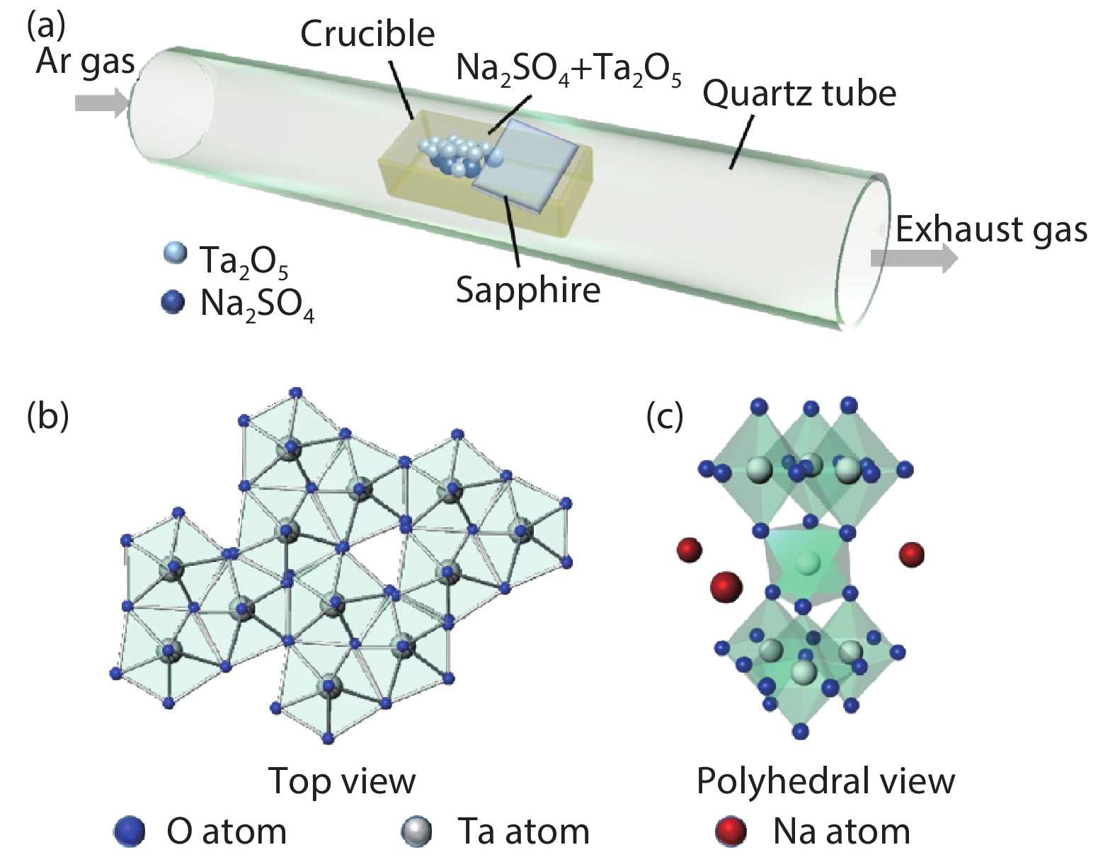
    Fig. 1. (Color online) Synthesis of thin Na2Ta4O11 flakes via CVD setup and crystal structure of Na2Ta4O11. (a) Schematic diagram of the CVD setup used for synthesis of Na2Ta4O11 flakes. (b) Top view of a single layer of TaO7 pentagonal bipyramids. (c) Polyhedral view of the local coordination environments in Na2Ta4O11 for a single TaO6 octahedron. The O, Ta and Na atoms are represented by blue, silver and red balls, respectively.
    (Color online) Characterizations of CVD-grown thin Na2Ta4O11 flakes. (a) Representative optical image. (b) AFM characterization. (c) XRD characterization. (d) Typical Raman spectra of Na2Ta4O11 flakes.
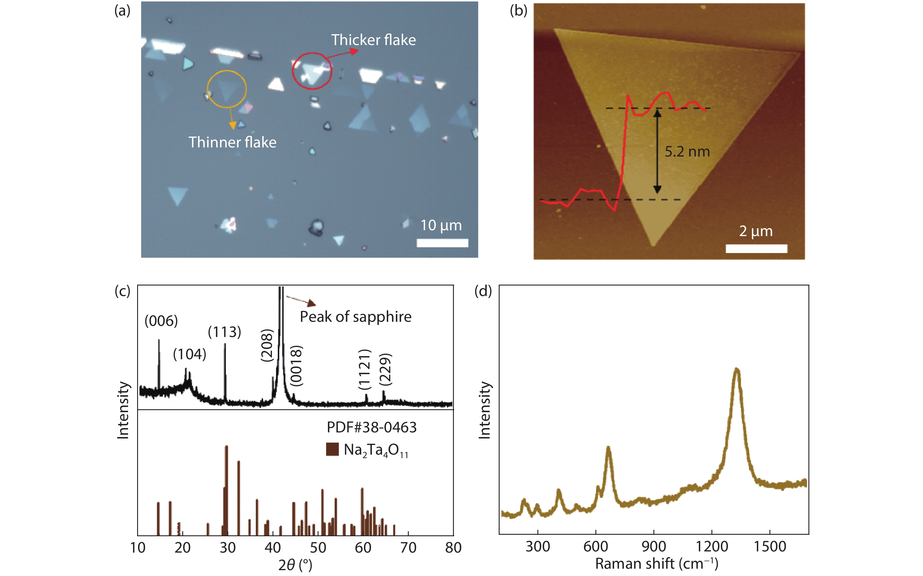
    Fig. 2. (Color online) Characterizations of CVD-grown thin Na2Ta4O11 flakes. (a) Representative optical image. (b) AFM characterization. (c) XRD characterization. (d) Typical Raman spectra of Na2Ta4O11 flakes.
    (Color online) Structure characterization of CVD-grown Na2Ta4O11 flakes on sapphire. XPS core level spectra of (a) Na 1s, (b) O 1s, and (c) Ta 4f. (d) HRTEM image and (e) FFT pattern image of thin Na2Ta4O11 flakes. (f) SEM image for analysis of EDS. (g) The corresponding EDS spectra of the Na2Ta4O11 flake in (f).
    Fig. 3. (Color online) Structure characterization of CVD-grown Na2Ta4O11 flakes on sapphire. XPS core level spectra of (a) Na 1s, (b) O 1s, and (c) Ta 4f. (d) HRTEM image and (e) FFT pattern image of thin Na2Ta4O11 flakes. (f) SEM image for analysis of EDS. (g) The corresponding EDS spectra of the Na2Ta4O11 flake in (f).
    (Color online) Deposition time-dependent optical images of Na2Ta4O11 flake. (a–d) Optical images of Na2Ta4O11 with deposition time at 30, 50, 60, and 90 min. Scale bars: 20 µm. (e–g) Representative AFM images of Na2Ta4O11 flake with deposition time from 30 to 60 min. (h) Average size (purple star) and thickness (blue square) as a function of growth time.
    Fig. 4. (Color online) Deposition time-dependent optical images of Na2Ta4O11 flake. (a–d) Optical images of Na2Ta4O11 with deposition time at 30, 50, 60, and 90 min. Scale bars: 20 µm. (e–g) Representative AFM images of Na2Ta4O11 flake with deposition time from 30 to 60 min. (h) Average size (purple star) and thickness (blue square) as a function of growth time.
    Yuanyuan Jin, Huimin Li, Song Liu. Growth of large-scale two-dimensional insulator Na2Ta4O11 through chemical vapor deposition[J]. Journal of Semiconductors, 2020, 41(7): 072901
    Download Citation