
Yuanyuan Jin, Huimin Li, Song Liu. Growth of large-scale two-dimensional insulator Na2Ta4O11 through chemical vapor deposition[J]. Journal of Semiconductors, 2020, 41(7): 072901
- Journal of Semiconductors
- Vol. 41, Issue 7, 072901 (2020)
Abstract
1. Introduction
The photocatalytic metal-oxides have attracted considerable attention thanks to their outstanding properties and applications. The solar power can be utilized to drive fuel-generating reactions, such as the photocatalytic water-splitting[
However, these methods have always produced impure crystal because they were grown in air, and the direct preparation of product in situ led to mixed reactants and products. Furthermore, these methods obtained either bulk Na2Ta4O11 crystals or small crystals. To date, there has been no study on the growth of thin-layered Na2Ta4O11, which will be essential to explore its optical properties. Chemical vapor deposition (CVD) is a powerful technology to synthesize large-scale two-dimensional (2D) materials. CVD is a process in which the chemical reactions between gaseous substances occurred, and subsequently produced solid sediments on the substrate[
Here, by using Na2SO4 and Ta2O5 as precursor, we first applied the CVD method to prepare large and thin-layered Na2Ta4O11 flake. The structure of Na2Ta4O11 flakes were characterized by X-ray diffraction (XRD), energy dispersive X-ray spectroscopy (EDS), and Raman techniques, indicating the successful synthesis of Na2Ta4O11. The atomic force microscope (AFM) demonstrated the thickness reached ~5.2 nm, which was the thinnest Na2Ta4O11 reported so far. High resolution transmission electron microscopy (HRTEM) revealed its high crystallinity and quality. Moreover, we observed that the growth time had strong effects on crystal size and thickness. Our work first synthesized thin-layer Na2Ta4O11, which paved the way for further exploration of its potential properties and applications.
2. Experiments
2.1. Growth of Na2Ta4O11
The growth was performed with a single temperature heating system, which was a 30 cm one-zone furnace system. Na2SO4 powder (14.2 mg, 99.5%, Sinopharm Chemical Reagent Co., Ltd) mixed with Ta2O5 powder (39.4 mg, 99.9%, Sigma Aldrich) were put into a crucible, which was placed at the highest temperature zone. A sapphire substrate was placed facedown above the mixed powders. Then the center of the furnace was heated to 850 °C for 43 min (the rate was 20 °C/min), which held for 30 min at 850 °C under 100 sccm high-purity (99.9999%) argon atmosphere. After growth, the tube was cooled naturally.
2.2. Characterization
SEM (Hitachi-S4800) combined with EDS was applied to characterize morphology and elemental composition. AFM (Bruker Dimension Icon) was used to measure the thickness. Raman analysis was conducted under the excitation of a 532 nm laser, which executed with an inVia confocal Renishaw Raman spectrometer. HRTEM (Tecnai G2 F20 S-TWIN) analysis was performed to investigate the structure on an atomic scale. The acceleration voltage was 60 kV to avoid damage samples. Element identification was acquired by using XPS (AXIS-165) equipped with a monochromatic Al Kα source (λ = 1486.6 eV). XRD (Bruker Dimension Icon D8 Advance system) measurements were performed by using Cu Kα radiation (40 kV, 40 mA).
3. Results and discussion
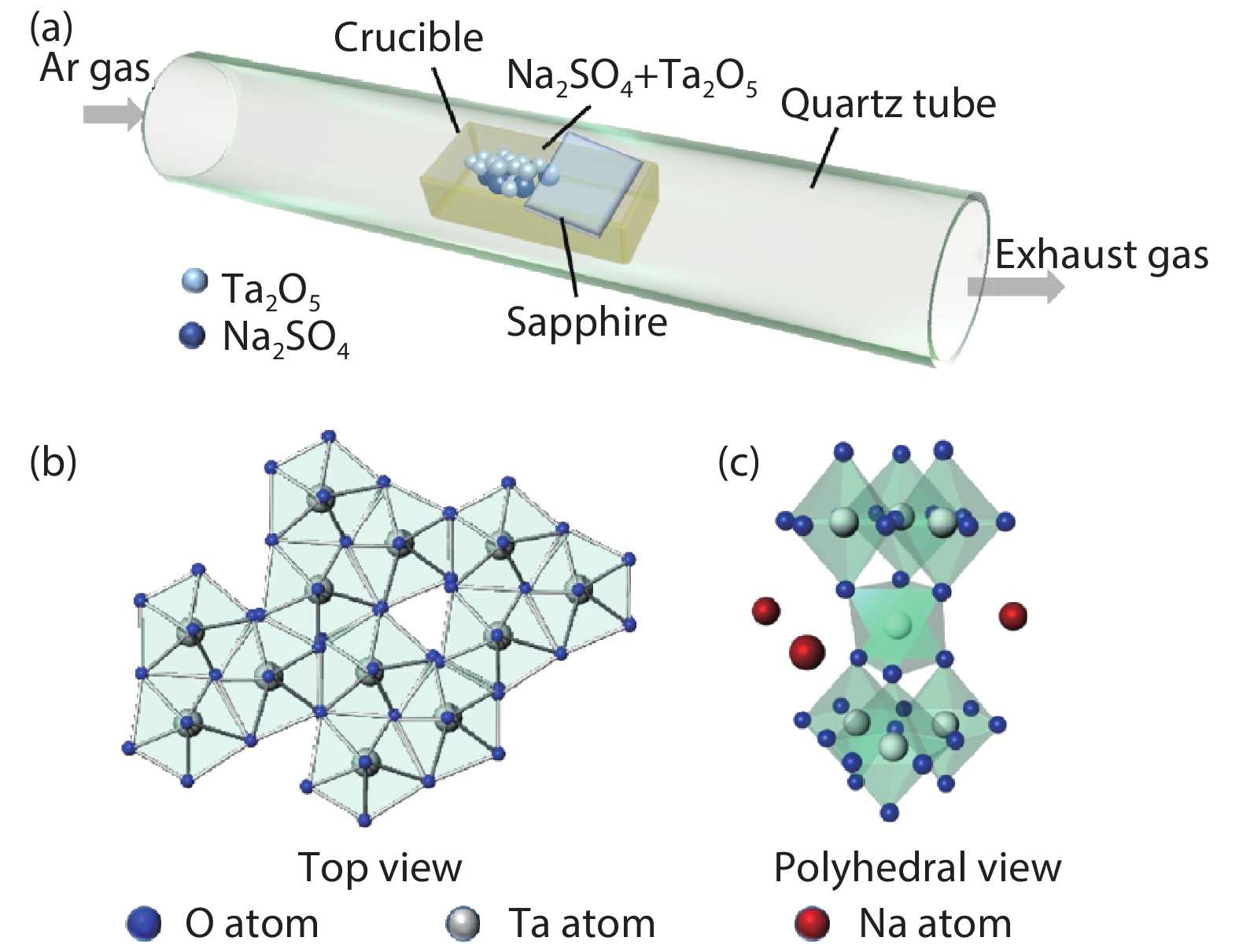
Fig. 1(a) illustrates the CVD setup. In brief, a crucible filled with mixture of Na2SO4 and Ta2O5 was placed in the center of heating zone. The corresponding molar ratio of precursors was 1 : 1. A sapphire substrate was loaded face down on top of the powder. Then, the heating zone was heated to 850 °C for 43 min (the rate was ~20 °C/min), which held for 30 min at 850 °C under 100 sccm high-purity (99.9999%) argon atmosphere. After growth, the furnace was cooled to room temperature. The growth details are depicted in the experimental section. The Na2Ta4O11 presented bilayer structure: a distort TaO7 pentagonal bipyramid layer, which alternated with another layer of isolated TaO6 octahedra[
![]()
Figure 1.(Color online) Synthesis of thin Na2Ta4O11 flakes via CVD setup and crystal structure of Na2Ta4O11. (a) Schematic diagram of the CVD setup used for synthesis of Na2Ta4O11 flakes. (b) Top view of a single layer of TaO7 pentagonal bipyramids. (c) Polyhedral view of the local coordination environments in Na2Ta4O11 for a single TaO6 octahedron. The O, Ta and Na atoms are represented by blue, silver and red balls, respectively.
Considering prior works, we deduced the reaction process between Na2SO4 and Ta2O5, involving two steps[
Typically, the as-grown Na2Ta4O11 flakes are triangles and hexagons. Fig. 2(a) displays the representative optical images of triangle Na2Ta4O11, in which the length of thin-layer flake was measured to be ~5.5 μm. It was obvious that each triangle flake showed a different color, revealing the varied thickness, in which the brighter triangles indicates thicker flakes and the darker ones represents thinner flakes (marked with red and yellow, respectively). Then, AFM was conducted to analyze the coarseness and height of representative thin flake (Fig. 2(b)). The height diagram revealed a thickness of ~5.2 nm, which was one of the smallest reported values. The corresponding AFM image indicated a flat and uniform surface of thin-layer Na2Ta4O11. Structure confirmation of Na2Ta4O11 was determined by XRD characterization (Fig. 2(c)), in which the result showed that positions of all diffraction peaks were consistent with the standard peaks of Na2Ta4O11. Strong and sharp peaks were observed, almost without the peaks of impurities, indicating the high crystallinity of Na2Ta4O11. It is noted that there is a strong peak at ~ 41.7°, which is assigned to the peak of the substrate of sapphire. Fig. 2(d) shows the Raman spectroscopy of Na2Ta4O11 excited with a 532 nm laser at room temperature. Six strong peaks are located at 224.5, 240.8, 294.8, 611, 661, and 1328.3 cm−1, respectively. The peak at 410 cm−1 belongs to the A1g mode of sapphire substrate. Although it was difficult to compare with other work due to the lack of previous studies about the Raman peak of Na2Ta4O11, we can still almost determine that these six strong peaks belong to the Na2Ta4O11 flake based on the confirmation of XRD.
![]()
Figure 2.(Color online) Characterizations of CVD-grown thin Na2Ta4O11 flakes. (a) Representative optical image. (b) AFM characterization. (c) XRD characterization. (d) Typical Raman spectra of Na2Ta4O11 flakes.
Figs. 3(a)–3(c) show the X-ray photoelectron spectroscopy (XPS) spectra of Na 1s, O 1s, and Ta 4f, ascertaining the state of each element in Na2Ta4O11. A strong single peak at 1071.9 eV is consistent with Na+ (Fig. 3(a))[
![]()
Figure 3.(Color online) Structure characterization of CVD-grown Na2Ta4O11 flakes on sapphire. XPS core level spectra of (a) Na 1s, (b) O 1s, and (c) Ta 4f. (d) HRTEM image and (e) FFT pattern image of thin Na2Ta4O11 flakes. (f) SEM image for analysis of EDS. (g) The corresponding EDS spectra of the Na2Ta4O11 flake in (f).
We then performed HRTEM technology to characterize the crystalline structure of flake, and the flake was transferred on TEM grid using the poly(methyl methacrylate) (PMMA)-assisted method[
These results demonstrate that the growth of thin-layer Na2Ta4O11 with CVD method worked extremely well. Of the governing parameters in this work, growth time was an important parameter for Na2Ta4O11 growth. At a growth temperature of 850 °C with molar ratio (Na2SO4 : Ta2O5) of 1 : 1, the growth time varied from 30 to 90 min. The optical images of flakes grown on sapphire corresponding to the deposition time of 30, 50, 60, and 90 min are presented in Figs. 4(a)–4(d). It is clear that the main morphology of Na2Ta4O11 flake is hexagonal and triangular. No substantial change of crystal size was shown before the growth time of 60 min. For longer growth time of 90 min, the interconnected Na2Ta4O11 flakes grow into a continuous film, which was measured to be 112 μm. At the boundary of the continuous film, we can observe several isolated triangles. This indicates that the formation of the film was initiated from the complete coalescence of flakes. Then AFM characterization was applied to measure the representative thickness of flakes grown at 30, 50, and 60 min, the results are shown in Figs. 4(e)–4(g). The AFM characterization of flakes at growth time of 90 min is not shown because of its height difference: it was thicker than the flakes obtained at a growth time of 60 min. These results can be evidenced by the color evolution of the Na2Ta4O11 flake. It is clear that the longer deposition time led to a thicker flake. Thickness increased with time without substantial size change before 60 min, which may result from the stronger chemical reactivity and lower energy barrier of Na2Ta4O11 surface when compared to the sapphire surface. Consequently, it resulted in a stack growth on thin Na2Ta4O11 flake surface instead of epitaxial lateral growth. The average size and thickness of Na2Ta4O11 as a function of growth time is illustrated in Fig. 4(h). In this case, the growth time of 60 min was a turning point to control the growth model of vertical stack growth and coalescence of flakes. We speculate that new seeding molecules were likely to deposit on the top of the bottom layer because of its low thermodynamic barrier on the surface. This barrier increased with thickness, thus Na2Ta4O11 molecules would tend to nucleate on the substrate surface and form new stacked grown Na2Ta4O11 flakes. Subsequently, adjacent Na2Ta4O11 flakes integrated with each other to form a large film.
![]()
Figure 4.(Color online) Deposition time-dependent optical images of Na2Ta4O11 flake. (a–d) Optical images of Na2Ta4O11 with deposition time at 30, 50, 60, and 90 min. Scale bars: 20
This study is the first work to grow large 2D Na2Ta4O11, which is important for researching its potential application and properties. The physical properties of Na2Ta4O11 change dramatically from three dimensional (3D) to 2D because electrons were confined to nanoscale motion in two dimensions[
4. Conclusion
In conclusion, thin Na2Ta4O11 flakes were first successfully prepared by the CVD method on sapphire substrate. The structure and growth of Na2Ta4O11 flakes were confirmed with comprehensive characterization approaches. Controllable thickness and size by regulating growth time gave evidence that the CVD method has advantages in controlling growth of Na2Ta4O11. This work is important for advancing the various technological applications of Na2Ta4O11, and it offers strategies to synthesize other non-layer metal oxide materials.
Acknowledgements
The work gratefully acknowledged financial support from the National Natural Science Foundation of China (Nos. 21975067, 21705036), Natural Science Foundation of Hunan Province, China (No. 2018JJ3035).
References
[1] M Machida, J I Yabunaka, T Kijima. Efficient photocatalytic decomposition of water with the novel layered tantalate RbNdTa2O7. Chem Commun, 30, 1939(1999).
[2] T Tanaka, H Nojima, T Yamamoto et al. Structure of surface tantalate species and photo-oxidation of carbon monoxide over silica-supported tantalum oxide. Phys Chem Chem Phys, 1, 5235(1999).
[3] S Suzuki, H Saito, K Yubuta et al. Growth of millimeter-sized platy single crystals of NaTaO3 from Na2MoO4 flux. Cryst Growth Des, 19, 3607(2019).
[4] I Ivanova, T A Kandiel, Y J Cho et al. Mechanisms of photocatalytic molecular hydrogen and molecular oxygen evolution over La-doped NaTaO3 particles: effect of different cocatalysts and their specific activity. ACS Catal, 8, 2313(2018).
[5] H Sudrajat, Y Zhou, T Sasaki et al. The atomic-scale structure of LaCrO3–NaTaO3 solid solution photocatalysts with enhanced electron population. Phys Chem Chem Phys, 21, 5148(2019).
[6] K Kishimoto, M Yoshio, T Mukai et al. Nanostructured anisotropic ion-conductive films. J Am Chem Soc, 125, 3196(2003).
[7] Y G Su, X Yang, T T Wang et al. Sol-gel synthesis of Na2Ta4O11 nanocrystals showing high efficient photocatalytic performance. Adv Mater Res, 1058, 35(2014).
[8] R Mattes, J Schaper. Crystal structure of Na2Ta4O11. Revue de Chimie Minerale, 22, 817(1985).
[9] et al. Template synthesized nano-crystalline natrotantite: preparation and photocatalytic activity for water decomposition. Mater Chem Physs, 110, 176(2008).
[10] N McLamb, P P Sahoo, L Fuoco et al. Flux growth of single-crystal Na2Ta4O11 particles and their photocatalytic hydrogen production. Cryst Growth Des, 13, 2322(2013).
[11] K Teshima, D Tomomatsu, T Suzuki et al. Growth of Na2Ta4O11 crystals from a Na2Mo2O7 flux. Cryst Growth Des, 6, 18(2006).
[12] Y Kim, S Kim, W H Lee et al. Direct transfer of CVD-grown graphene onto eco-friendly cellulose film for highly sensitive gas sensor. Cellulose, 27, 1685(2020).
[13] D Kumar, R K Ghadai, S Das et al. Effect of nitrogen flow rate on the mechanical properties of CVD-deposited SiCN thin films. Bull Mater Sci, 42, 251(2019).
[14] Y Jin, Z Zeng, Z Xu et al. Synthesis and transport properties of degenerate p-type Nb-doped WS2 monolayers. Chem Mater, 31, 3534(2019).
[15] K C Kwon, C Kim, Q V Le et al. Synthesis of atomically thin transition metal disulfides for charge transport layers in optoelectronic devices. ACS Nano, 9, 4146(2015).
[16] K Y Ko, S Lee, K Park et al. High-performance gas sensor using a large-area WS2
[17] S Wang, Y Rong, Y Fan et al. Shape evolution of monolayer MoS2 crystals grown by chemical vapor deposition. Chem Mater, 26, 6371(2014).
[18] M Harb, D Masih, S Ould-Chikh et al. Determination of the electronic structure and UV–Vis absorption properties of (Na2–
[19] O Palasyuk, A Palasyuk, P A Maggard. Site-differentiated solid solution in (Na1−
[20] M Mobin, A Malik. Studies on the interactions of transition metal oxides and sodium sulfate in the temperature range 900–1200 K in oxygen. J Alloy Compd, 235, 97(1996).
[21] M A Muñoz-Márquez, M Zarrabeitia, E Castillo-Martínez et al. Composition and evolution of the solid-electrolyte interphase in Na2Ti3O7 electrodes for Na-ion batteries: XPS and auger parameter analysis. ACS Appl Mater Interfaces, 7, 7801(2015).
[22] K Kotsis, V Staemmler. Ab initio calculations of the O1s XPS spectra of ZnO and Zn oxo compounds. Phys Chem Chem Phys, 8, 1490(2006).
[23] R Grilli, R Simpson, C Mallinson et al. Comparison of Ar+ monoatomic and cluster ion sputtering of Ta2O5 at different ion energies, by XPS: Part 2-cluster ions. Surf Sci Spectra, 21, 68(2014).
[24] H Van Ngoc, Y Qian, S K Han et al. PMMA-etching-free transfer of wafer-scale chemical vapor deposition two-dimensional atomic crystal by a water soluble polyvinyl alcohol polymer method. Sci Rep, 6, 33096(2016).
[25] S Ithurria, D V Talapin. Colloidal atomic layer deposition (c-ALD) using self-limiting reactions at nanocrystal surface coupled to phase transfer between polar and nonpolar media. J Am Chem Soc, 134, 18585(2012).

Set citation alerts for the article
Please enter your email address
© Copyright 2018-2021 | Chinese Laser Press. All Rights Reserved 沪ICP备15018463号-20