• Journal of Semiconductors
  • Vol. 41, Issue 11, 111404 (2020)
Xing Li1、2 and Lei Zhou2
Author Affiliations
  • 1University of Chinese Academy of Sciences, Beijing 100049, China
  • 2Institute of Microelectronics of Chinese Academy of Sciences, Beijing 100029, China
  • show less
    DOI: 10.1088/1674-4926/41/11/111404 Cite this Article
    Xing Li, Lei Zhou. A survey of high-speed high-resolution current steering DACs[J]. Journal of Semiconductors, 2020, 41(11): 111404 Copy Citation Text show less
    (Color online) Performance comparison of state-of-the-art DACs: SFDR@1GHz vs. sampling rate.
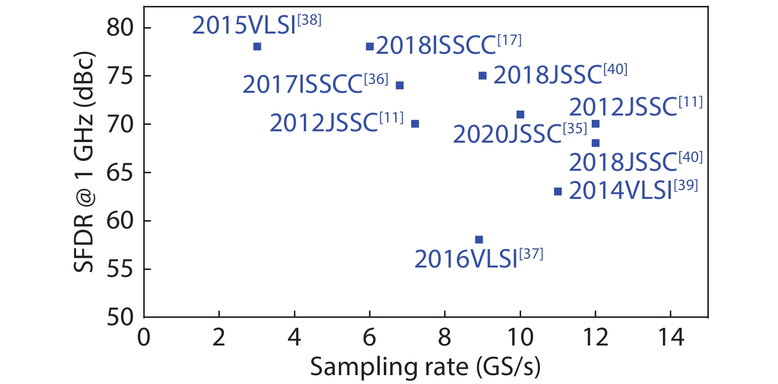
    Fig. 1. (Color online) Performance comparison of state-of-the-art DACs: SFDR@1GHz vs. sampling rate.
    (Color online) Performance comparison of state-of-the-art DACs: (a) FoM1, (b) FoM2, (c) FoM3 versus sampling rate.
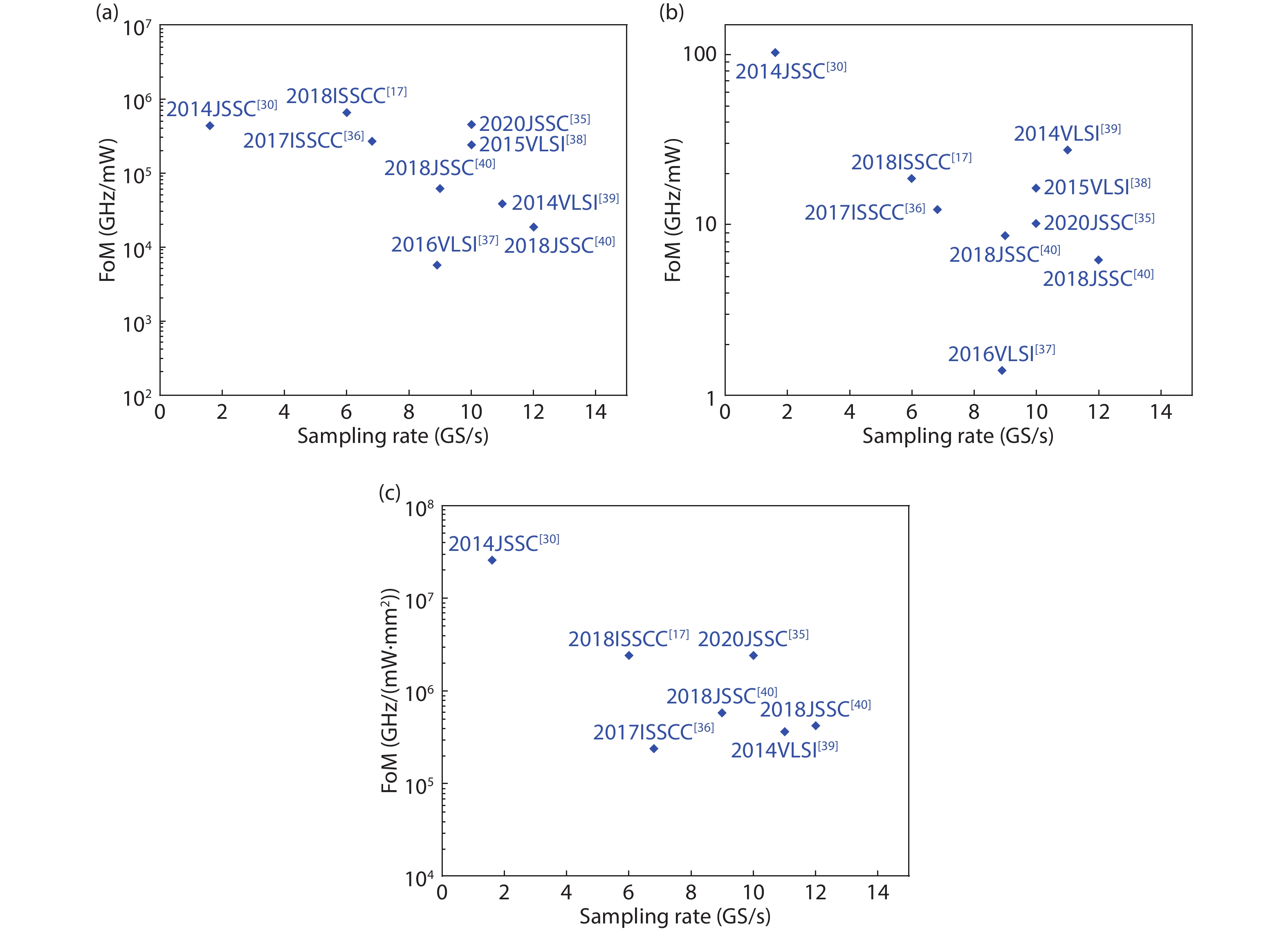
    Fig. 2. (Color online) Performance comparison of state-of-the-art DACs: (a) FoM1, (b) FoM2, (c) FoM3 versus sampling rate.
    (Color online) Block diagram of a high-speed high-resolution current steering DAC with a typical switching current cell.
    Fig. 3. (Color online) Block diagram of a high-speed high-resolution current steering DAC with a typical switching current cell.
    A typical switching current cell proposed in Ref. [21].
    Fig. 4. A typical switching current cell proposed in Ref. [21].
    Quad-switching current cell with switch cascodes reported in Ref. [38].
    Fig. 5. Quad-switching current cell with switch cascodes reported in Ref. [38].
    A simplified quad-switch cell proposed in Ref. [34].
    Fig. 6. A simplified quad-switch cell proposed in Ref. [34].
    RZ current cell with resampling switches proposed in Ref. [11].
    Fig. 7. RZ current cell with resampling switches proposed in Ref. [11].
    (Color online) Magnitude of the frequency response for NRZ, RZ, and MRZ waveforms reported in Ref. [53].
    Fig. 8. (Color online) Magnitude of the frequency response for NRZ, RZ, and MRZ waveforms reported in Ref. [53].
    A typical fast latch proposed in Ref. [21]
    Fig. 9. A typical fast latch proposed in Ref. [21]
    High-speed latch presented in Ref. [57].
    Fig. 10. High-speed latch presented in Ref. [57].
    DAC output stack, with the switch driver proposed in Ref. [37].
    Fig. 11. DAC output stack, with the switch driver proposed in Ref. [37].
    Block diagram of dummy trigger proposed in Ref. [56].
    Fig. 12. Block diagram of dummy trigger proposed in Ref. [56].
    Master-slave latch presented in Ref. [58].
    Fig. 13. Master-slave latch presented in Ref. [58].
    Double-edge current switch driver with enhanced reset circuit reported in Ref. [59].
    Fig. 14. Double-edge current switch driver with enhanced reset circuit reported in Ref. [59].
    Two-parameter calibration loop configuration and CAL_DACs proposed in Ref. [28].
    Fig. 15. Two-parameter calibration loop configuration and CAL_DACs proposed in Ref. [28].
    Conceptual block diagram of a dual-rate hybrid DAC architecture proposed in Ref. [49].
    Fig. 16. Conceptual block diagram of a dual-rate hybrid DAC architecture proposed in Ref. [49].
    OIC technique with compensation resistor proposed in Ref. [35].
    Fig. 17. OIC technique with compensation resistor proposed in Ref. [35].
    ParameterRef. [4] Ref. [11] Ref. [17] Ref. [30] Ref. [35] Ref. [36] Ref. [37] Ref. [38] Ref. [39] Ref. [40]
    Process (nm)281301640281640652865
    Resolution (bit)1314/12161214141416916
    Sampling rate (GS/s)97.2/1261.6106.88.910119/12
    SFDR@Nyquist frequency (dBc)N/A67/55677065625069 @3GS/s5156/52
    IM3@DC-Nyquist frequency (dBc)<–45N/A<–82<–70<–70<–71<–65<–73 @3GS/s<–51<–67/<–67
    NSD (dBm/Hz)N/A–161/–159–162 @2.6GHz–150 @800MHz–158 @5GHz–160N/AN/AN/A–130 @6GHz
    Power (mW)360N/A350401623301200800110758/1065
    Area (mm2) 1.16N/A0.520.0160.070.855N/AN/A0.040.97
    FoM1 (GHz/mW)N/AN/A6.5×1054.4×1054.5×1052.7×1055.6×1032.5×1053.8×1046.3×104/ 1.9×10⁴
    FoM2 (GHz/mW)N/AN/A18.7102.410.112.41.416.427.98.6/6.2
    FoM3(GHz/(mW·mm2)) N/AN/A2.4×1062.6×1072.4×1062.4×105N/AN/A3.6×1055.8×105/ 4.2×10⁵
    Table 1. Performance summary and comparison with state-of-the-art high-speed high-resolution DACs.
    FoM1FoM2FoM3
    Definition
    Reference[30] [41] [42]
    ExplanationSFDRBest/SFDRworst: Best/Worst measured SFDR in whole Nyquist bandwidth; fclk: Sampling rate; Ptotal/Pload: Power consumption of the whole DAC/load; N: Resolution; fs@6(N–1): Output signal frequency where the SFDR has dropped with 6 dB (= 1 bit) in comparison with the expected result (≈ 6N) (Note: If the measured SFDR cannot reach 6(N–1), 0.1 GHz is selected here for calculation); Area: The core area of the DAC.
    Table 2. Detailed definitions of DAC FoMs.
    ParameterINL at 40 °C (14-bit level LSB)DNL at 40 °C (14-bit level LSB)Temperature drift 1σ (LSB)
    No CAL6.023.331.6
    Ref. [24] 0.200.161.6
    Ref. [27] 0.230.160.8
    Ref. [28] N/AN/A0.6
    Table 3. INL, DNL and temperature drift summary of proposed foreground calibration techniques.
    Xing Li, Lei Zhou. A survey of high-speed high-resolution current steering DACs[J]. Journal of Semiconductors, 2020, 41(11): 111404
    Download Citation