
Xing Li, Lei Zhou. A survey of high-speed high-resolution current steering DACs[J]. Journal of Semiconductors, 2020, 41(11): 111404
- Journal of Semiconductors
- Vol. 41, Issue 11, 111404 (2020)
Abstract
1. Introduction
Digital to analog converters (DAC) are circuits that converse signals with information in bits to signals with information in their amplitude and time domain characteristics[
Due to the increasing demand for higher data rates, transmitters[
In the design of current steering DACs, the main challenge is to reduce the impact of static and dynamic errors. The static errors mainly come from the amplitude mismatch of current sources[
As the sampling rate and signal frequency increases, the dynamic errors begin to dominate. The dynamic errors include finite output impedance[
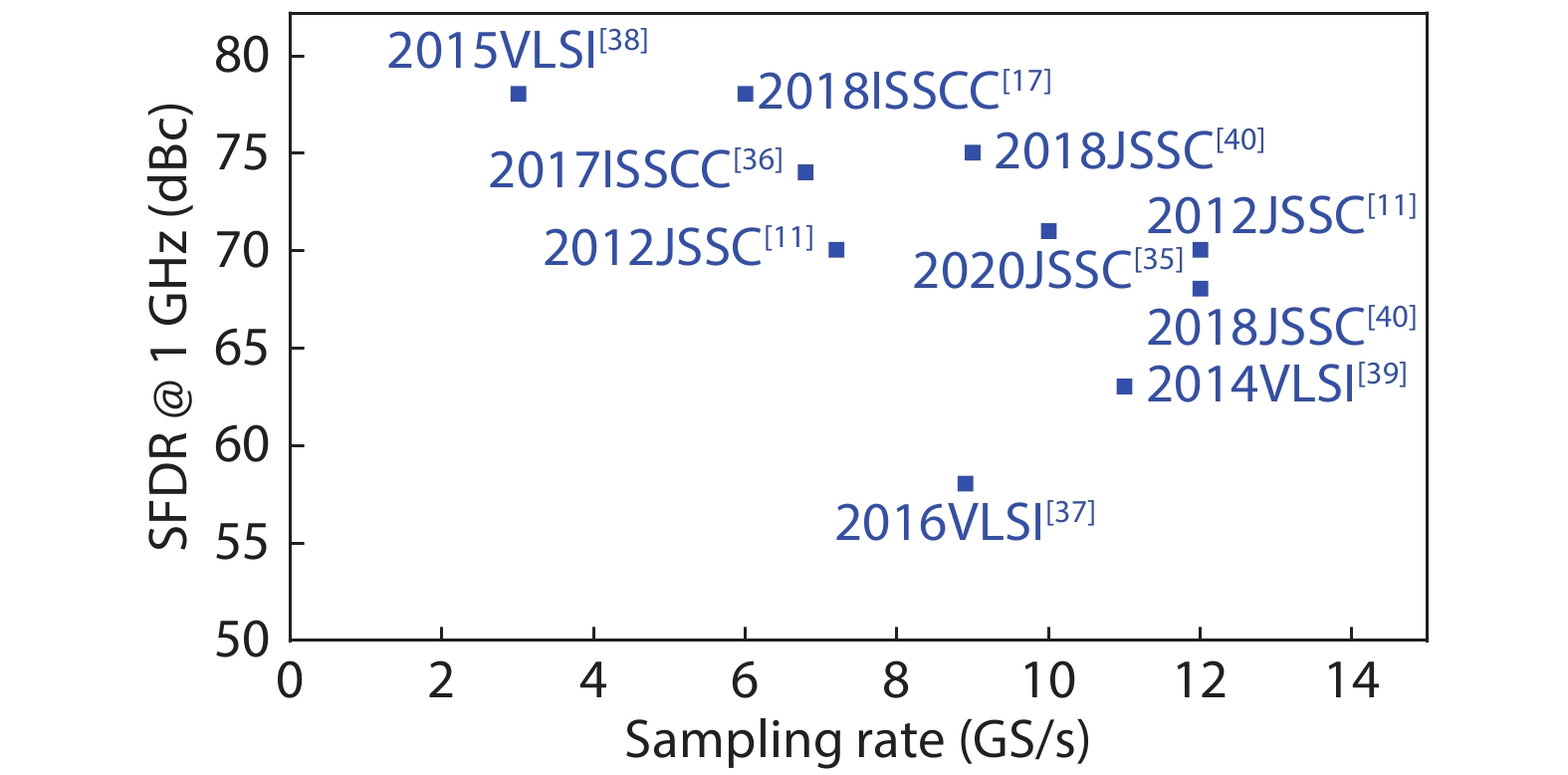
With the continuous development of IC design and process technology, a series of high-speed high-resolution DACs have been reported with a higher sampling rate, higher resolution, better performance, and lower power consumption. In Fig. 1, a comparison is made with the spurious free dynamic range (SFDR) performance versus sampling rate of high-speed high-resolution DACs published in the top conferences and journals in recent years.
![]()
Figure 1.(Color online) Performance comparison of state-of-the-art DACs: SFDR@1GHz vs. sampling rate.
Table 1 shows a more detailed performance summary and comparison with these state-of-the-art high-speed high-resolution current steering DACs. Figs. 2(a)–2(c) show the comparison of three common figures of merit (FoM) versus sampling rate with detailed definitions of the FoMs are given in Table 2.
![]()
Figure 2.(Color online) Performance comparison of state-of-the-art DACs: (a) FoM1, (b) FoM2, (c) FoM3 versus sampling rate.
Table Infomation Is Not EnableThis paper aims to provide a survey of cutting-edge high-speed high-resolution DACs with the mainstream technologies in circuit implementations. The rest of this paper is organized as follows. Section 2 presents a roughly description about the architecture of the current steering DACs. Section 3 outlines the dominating techniques in the subcircuit design, including the encoding segmentation, switching current source and the switch driver. Section 4 introduces the calibration and error reducing techniques for static and dynamic errors. The summary is given in Section 5.
2. Architecture of high-speed high-resolution DACs
The block diagram of a traditional high-speed high-resolution current steering DAC is shown in Fig. 3. In such an architecture, the input digital signal (binary bits) can be covert into unary bits by the thermometer encoder, or go through a delay equalizer to align the data stream for the segmented encoding. If a higher sampling rate is needed, multiplexers (MUX) can be introduced before or after the encoder[
![]()
Figure 3.(Color online) Block diagram of a high-speed high-resolution current steering DAC with a typical switching current cell.
3. Subcircuit design
3.1. Encoding and segmentation
Encoder is one of the critical subcircuits. As mentioned before, a suitable encoding method is important for higher linearity design. According to the different current weights of current-steering cells, there are three encoding architectures of current steering DAC: binary-weighted architecture[
Since the digital input of DAC is binary codes, the binary-weighted architecture is the most intuitive way. Refs. [18, 20] reveal that the advantages of this architecture are its simplicity. However, with the increase of N (resolution), the MSB-controlled current source differs greatly from the current source controlled by the least significant bits (LSB). To be precise, the maximum current is 2N–1 times that of the minimum current[
The thermometer-weighted (unary-weighted) architecture is another option, which means that all switching currents have the same weight. This architecture can bring less disturbances on the output signal[
Generally speaking, the segmented architecture is the preferred one to combine the advantages of above architectures: the coarse bits use thermometer-type coding to reduce the requirements on matching and improve the linearity, while the fine bits using binary coding to reduce the complexity of current cells. As a result, the most important trade-off is the segment ratio[
Large coarse bits will introduce more parasitic capacitance, while large fine bits bringing the mismatch of current cells at the border. In Ref. [47], a design procedure of segmentation is outlined. The matching accuracy of the current source can be estimated based on the size of the transistors. After that, the maximum number of LSB section is determined according to the estimation and the yield requirements. Ref. [49] builds a model with the bandwidth and SFDR represented as a function of segmentation ratio for its hybrid DAC. Ref. [17] chooses a 6–10 segmentation in combination with the bounded INL calibration for a 16-bit DAC. In Ref. [35], the incoming data is decoded to the 3–3–3–5 (unary–unary–unary–binary) segmentation for a compact layout. In short, the segmentation design is not constant for a specific resolution, a compromise between good static and dynamic specifications versus power and area should be found[
3.2. Switching current source cell design
In current steering DACs, the performance of switching current source determines the performance of the DAC. A typical structure of the switching current source cell is shown in Fig. 4, which contains a cascoded current source, differential current switches, thick-oxide output cascodes and bleeding currents[
![]()
Figure 4.A typical switching current cell proposed in Ref. [
As discussed earlier, the finite output impedance of the current source is one of the important factors that affect the dynamic performance. For this reason, the thick-oxide cascode devices (M4/M5) are added between the switch (M2/M3) and the output node to reduce the effect at low frequencies[
![]()
Figure 5.Quad-switching current cell with switch cascodes reported in Ref. [
In the design of switching current source cell, it is crucial to reduce the signal-dependence of switch behavior[
Ref. [34] proposed a quad-switch as presented in Fig. 6, using two pairs of differential switches, which are activated alternately in every clock cycle. Even if there is no data change, the switching event will occur. The code-independent switching event improves the distortion performance at high frequency. Engel et al.[
![]()
Figure 6.A simplified quad-switch cell proposed in Ref. [
RZ switch is also an effective method to reduce the signal-dependent nonlinearity, as it can insert a zero output state between two consecutive signals[
![]()
Figure 7.RZ current cell with resampling switches proposed in Ref. [
![]()
Figure 8.(Color online) Magnitude of the frequency response for NRZ, RZ, and MRZ waveforms reported in Ref. [
3.3. Switch driver circuit design
The switch driver is the transition cell from the digital domain to the analog domain[
Ref. [21] proposed a typical switch gate driving, which creates a steep transition and has a short clock-to-output delay. This structure, as shown in Fig. 9, is also applied in Refs. [2, 56]. This pseudo-differential CMOS latch has advantages on driving the analog current source cell directly, and providing the final timing for the data input of the current source cells. To accelerate the signal transition further, PMOS transistors are added in Ref. [57], getting the capability of both pull-up and pull-down. The simplified schematic of the high-speed latch is demonstrated in Fig. 10, while the similar structure demonstrated in Fig. 11 may produce faster rise/fall times owing to the devices M1–M4[
![]()
Figure 9.A typical fast latch proposed in Ref. [
![]()
Figure 10.High-speed latch presented in Ref. [
![]()
Figure 11.DAC output stack, with the switch driver proposed in Ref. [
For the switch driver design, a critical problem is the mismatch of the signal-dependent switching timing. The latches driving the current source cells are intrinsically nonstatic, and the signal generated by the final latches will produce supply ripples[
![]()
Figure 12.Block diagram of dummy trigger proposed in Ref. [
Erdmann et al.[
Ravinuthula et al.[
In addition, the CML latch configuration is commonly used for low-swing differential operation at high frequencies and small disturbance on the power supply. A master–slave CML latch was applied in Ref. [58]. The digital output of the encoder will be latched first by master latches, then by slave latches, as shown in Fig. 13. The usage of two latch stages enables precise timing and steep edges to minimize the timing errors. The double-edge switch driver can be introduced to reduce the input clock frequency, and one of its major drawbacks is the memory effect, or the inter-symbol interference (ISI). Since the last operation may affect the next working state, Ref. [59] adds reset transistors to the common source node of the CML switch driver to form an enhanced reset circuit in a 14-bit 8GS/s DAC. As depicted in Fig. 14, when one branch is in off state, the associated reset transistor charges the common node to a fixed voltage.
![]()
Figure 13.Master-slave latch presented in Ref. [
![]()
Figure 14.Double-edge current switch driver with enhanced reset circuit reported in Ref. [
4. Calibration and error reducing techniques
4.1. Static error calibration techniques
In current steering DACs, the main goal of static error calibration is reducing the amplitude mismatch between current sources.
Calibration techniques can be divided into foreground calibration[
While the foreground calibration is performed only once, the background retriggers the current cell periodically. It not only eliminates the static mismatch, but also tracks the error slow varying with time, which is related to the bias conditions and chip temperature fluctuations[
Another attractive option for static error calibration is the foreground calibration technique. A successive approximation register (SAR) logic and a CAL_DAC can be introduced[
The main constraints of the foreground calibration techniques are their sensitivity to the temperature and supply voltage variations. To track the current source mismatch change with temperature, Zhu et al.[
where I is the nominal bias current and
However, the scheme explained above only considers the main component of the mismatch current. For greater accuracy, Zhu et al.[
![]()
Figure 15.Two-parameter calibration loop configuration and CAL_DACs proposed in Ref. [
4.2. Dynamic error reducing techniques
With the improvement of the sampling rate and output bandwidth, the dynamic errors become more dominant on the high frequency performance. The DEM technique[
DEM technique is an effective technique which can suppress both static and dynamic errors. Its principle is to select the circuit cell by randomization, which refers to the random permutation of switches[
RZ technique has been mentioned in Section 3.2, which means that the output tracks the signal once it has settled and then returns to zero. A typical RZ switching current cell was presented in Fig. 7 and the ideal RZ output is a square waveform composed of the signal value and zero in a clock cycle[
DEM and DRZ can be used in combination[
The layout arrangement technique is also a significant option to mitigate the systematic matching errors. To reduce the timing skew induced between current cells, Ref. [35] applied the Q2 random walk arrangement with a common centroid proposed in Ref. [64], and then described a novel method named concentric parallelogram routing (CPR). The routing lengths used to connect the sub-cells can be equal, achieving a lower gradient mismatch error. In Ref. [53], a vertically stacked tree (VST) structure forms an H-tree for each cell was proposed to provide identical path lengths to the output summing node, thereby minimizing variations in amplitude and phase.
A number of excellent dynamic error reducing techniques are proposed in recent years. To break the linearity limitation of Nyquist DAC, a hybrid DAC architecture with a Nyquist path and an oversampling path was proposed by Su et al.[
![]()
Figure 16.Conceptual block diagram of a dual-rate hybrid DAC architecture proposed in Ref. [
To mitigate the data-dependent switching distortions, a random pairwise swapping (RPS) technique was proposed in Ref. [68], which reduces the intermodulation distortions between the element transition rate and the output-dependent unit switching. RPS randomly swaps the switching control signals of paired switching units in the random DEM decoding, resulting a 5–12 dB SFDR improvement at 1.0 GS/s.
To remedy the finite output impedance effect at high frequencies, an output impedance compensation (OIC) technique was proposed in Ref. [35], which introduces a data-dependent compensation resistor, Rcp(Din). The current induced by the Rcp changes the current through the load resistors for compensating the distortion. The Rcp can be approximated by a PMOS biased with a data-dependent gate voltage VG(Din), as shown in Fig. 17. Notably, the OIC technique enables the use of non-cascoded current cells. A 14-bit 10 GS/s DAC with > 65 dBc SFDR over the entire Nyquist bandwidth was achieved by using the simple PMOS-based Rcp(Din) with two-level VG(Din).
![]()
Figure 17.OIC technique with compensation resistor proposed in Ref. [
5. Conclusion
Nowadays high-speed high-resolution DACs have been widely applied. In 5G communication, optical communication, and more broadband applications, the DAC becomes a bottleneck that limits the performance of the system. The state-of-the-art high-speed high-resolution current steering DACs are reviewed in this paper, with focus on the subcircuit design and error reducing techniques. Comparisons are made between different architectures, circuit implementations and calibration techniques along with three common FoM results.
References
[1]
[2] S Spiridon, J Tang, H Yan et al. A 375 mW multimode DAC-based transmitter with 2.2 GHz signal bandwidth and in-band IM3 < –58 dBc in 40 nm CMOS. IEEE J Solid State Circuits, 48, 1595(2013).
[3]
[4] J Xiao, B Chen, T K Kim et al. A 13-bit 9GS/s RF DAC-based broadband transmitter in 28nm CMOS. IEEE Symposium on VLSI Circuits, 262(2013).
[5] P C Ku, K Y Shih, L H Lu. A high-voltage DAC-based transmitter for coded signals in high frequency ultrasound imaging applications. IEEE Trans Circuits Syst I, 65, 2797(2018).
[6] C Erdmann, B Verbruggen, B Vaz et al. A modular 16nm direct-RF TX/RX embedding 9GS/S DAC and 4.5GS/S ADC with 90dB isolation and sub-80PS channel alignment for monolithic integration in 5G base-station SoC. 2018 IEEE Symposium on VLSI Circuits, 219(2018).
[7]
[8] A Roshan-Zamir, B Wang, S Telaprolu et al. A two-segment optical DAC 40 Gb/s PAM4 silicon microring resonator modulator transmitter in 65nm CMOS. IEEE Optical Interconnects Conference (OI), 5(2017).
[9] W Z Li, L Zhou, M Luo et al. 100Gb/s/λ optical fiber transmission based on high speed DAC in SiGe technology. 2018 Conference on Lasers and Electro-Optics Pacific Rim, 1(2018).
[10] P Ostrovskyy, O Schrape, K T Helmric et al. A radiation hardened 16 GS/s arbitrary waveform generator ic for a submillimeter wave chirp-transform spectrometer. 2018 IEEE Nordic Circuits and Systems Conference (NORCAS): NORCHIP and International Symposium of System-on-Chip (SoC), 1(2018).
[11] F Van de Sande, N Lugil, F Demarsin et al. A 7.2 GSa/s, 14 bit or 12 GSa/s, 12 bit signal generator on a chip in a 165 GHz
[12]
[13] Y Zhuang, B Magstadt, T Chen et al. High-purity sine wave generation using nonlinear DAC with predistortion based on low-cost accurate DAC–ADC co-testing. IEEE Trans Instrum Meas, 67, 279(2018).
[14] J S Hansen, G Jue. New approach to spectrum and emitter simulation: For the evaluation of radar and electronic warfare systems. 2013 International Conference on Radar, 532(2013).
[15] A Glascott-Jones, N Chantier, F Bore et al. Direct conversion to X band using a 4.5 GSps SiGe digital to analog converter. 2014 International Radar Conference, 1(2014).
[16] Y Yao, F Dai, R C Jaeger et al. A 12-bit cryogenic and radiation-tolerant digital-to-analog converter for aerospace extreme environment applications. IEEE Trans Ind Electron, 55, 2810(2008).
[17] C H Lin, K L J Wong, T Y Kim et al. A 16b 6GS/S Nyquist DAC with IMD < –90dBc up to 1.9GHz in 16nm CMOS. 2018 IEEE International Solid-State Circuits Conference (ISSCC), 360(2018).
[18] A van den Bosch, M A F Borremans, M S J Steyaert et al. A 10-bit 1-GSample/s Nyquist current-steering CMOS D/A converter. IEEE J Solid-State Circuits, 36, 315(2001).
[19] B C Kim, M H Cho, Y G Kim et al. A 1 V 6-bit 2.4 GS/s Nyquist CMOS DAC for UWB systems. 2010 IEEE MTT-S International Microwave Symposium, 912(2010).
[20] F T Chou, C M Chen, Z Y Chen et al. A novel glitch reduction circuitry for binary-weighted DAC. 2014 IEEE Asia Pacific Conference on Circuits and Systems (APCCAS), 240(2014).
[21] C H Lin, F M L van der Goes, J R Westra et al. A 12 bit 2.9 GS/s DAC with IM3 < < –60 dBc beyond 1 GHz in 65 nm CMOS. IEEE J Solid-State Circuits, 44, 3285(2009).
[22] Y H Gong, R L Geiger. Switching sequence optimization for gradient error compensation in thermometer-decoded DAC arrays. IEEE Trans Circuits Syst II, 47, 585(2000).
[23] H Chen, L Y Liu, D M Li et al. A 12-bit current steering DAC with 2-dimensional gradient-error tolerant switching scheme. J Semicond, 31, 105006(2010).
[24] D A Mercer. Low-power approaches to high-speed current-steering digital-to-analog converters in 0.18-
[25] H H Chen, J Lee, J Weiner et al. A 14-b 150 MS/s CMOS DAC with digital background calibration. 2006 Symposium on VLSI Circuits, 51(2006).
[26] M Clara, W Klatzer, B Seger et al. A 1.5V 200MS/s 13b 25mW DAC with randomized nested background calibration in 0.13
[27]
[28] H Y Zhu, W H Yang, G Engel et al. A two-parameter calibration technique tracking temperature variations for current source mismatch. IEEE Trans Circuits Syst II, 64, 387(2017).
[29] S H Xu, J W Lee. Calibration and correction of timing mismatch error in two-channel time-interleaved DACs. 2019 IEEE International Symposium on Circuits and Systems (ISCAS), 1(2019).
[30] W T Lin, H Y Huang, T H Kuo. A 12-bit 40 nm DAC achieving SFDR > 70 dB at 1.6 GS/s and IMD –61dB at 2.8 GS/s with DEMDRZ technique. IEEE J Solid-State Circuits, 49, 708(2014).
[31]
[32] E Bechthum, G I Radulov, J Briaire et al. A wideband RF mixing-DAC achieving IMD < –82 dBc up to 1.9 GHz. IEEE J Solid-State Circuits, 51, 1374(2016).
[33] S Su, M S Chen. A 12-Bit 2 GS/s dual-rate hybrid DAC with pulse-error predistortion and in-band noise cancellation achieving > 74 dBc SFDR and < –80 dBc IM3 up to 1 GHz in 65 nm CMOS. IEEE J Solid-State Circuits, 51, 2963(2016).
[34] S Park, G Kim, S C Park et al. A digital-to-analog converter based on differential-quad switching. IEEE J Solid-State Circuits, 37, 1335(2002).
[35] H Huang, T Kuo. A 0.07-mm2 162-mW DAC achieving > 65 dBc SFDR and < –70 dBc IM3 at 10 GS/s with output impedance compensation and concentric parallelogram routing. IEEE J Solid-State Circuits, 55, 2478(2020).
[36] C Erdmann, E Cullen, D Brouard et al. A 330mW 14b 6.8GS/s dual-mode RF DAC in 16nm FinFET achieving –70.8dBc ACPR in a 20MHz channel at 5.2GHz. 2017 IEEE International Solid-State Circuits Conference (ISSCC), 280(2017).
[37] V Ravinuthula, W Bright, M Weaver et al. A 14-bit 8.9GS/s RF DAC in 40nm CMOS achieving >71dBc LTE ACPR at 2.9GHz. 2016 IEEE Symposium on VLSI Circuits (VLSI-Circuits), 1(2016).
[38]
[39]
[40] S Y Su, M S W Chen. A 16-bit 12-GS/s single-/dual-rate DAC with a successive bandpass delta-sigma modulator achieving <–67-dBc IM3 within DC to 6-GHz tunable passbands. IEEE J Solid-State Circuits, 53, 3517(2018).
[41]
[42]
[43] A Nazemi, K M Hu, B Catli et al. 3.4 A 36Gb/s PAM4 transmitter using an 8b 18GS/S DAC in 28nm CMOS. 2015 IEEE International Solid-State Circuits Conference (ISSCC), 1(2015).
[44] Y M Greshishchev, D Pollex, S C Wang et al. A 56GS/S 6b DAC in 65nm CMOS with 256×6b memory. 2011 IEEE International Solid-State Circuits Conference, 194(2011).
[45] J P Carreira. A two-step flash ADC for digital CMOS technology. Second International Conference on Advanced A-D and D-A Conversion Techniques and their Applications, 48(1994).
[46]
[47] C H Lin, K Bult. A 10-b, 500-MSample/s CMOS DAC in 0.6 mm2. IEEE J Solid-State Circuits, 33, 1948(1998).
[48]
[49] S Y Su, T I Tsai, P K Sharma et al. A 12 bit 1 GS/s dual-rate hybrid DAC with an 8 GS/s unrolled pipeline delta–sigma modulator achieving > 75 dB SFDR over the nyquist band. IEEE J Solid-State Circuits, 50, 896(2015).
[50] B Schafferer, R Adams. A 3V CMOS 400mW 14b 1.4GS/s DAC for multi-carrier applications. 2004 IEEE International Solid-State Circuits Conference, 360(2004).
[51] A R Bugeja, B S Song, P L Rakers et al. A 14-b, 100-MS/s CMOS DAC designed for spectral performance. IEEE J Solid-State Circuits, 34, 1719(1999).
[52] M J Choe, K H Baek, M Teshome. A 1.6-GS/s 12-bit return-to-zero GaAs RF DAC for multiple Nyquist operation. IEEE J Solid-State Circuits, 40, 2456(2005).
[53] L Duncan, B Dupaix, J J McCue et al. A 10-bit DC-20-GHz multiple-return-to-zero DAC with >48-dB SFDR. IEEE J Solid-State Circuits, 52, 3262(2017).
[54]
[55]
[56]
[57] X Q Li, Q Wei, Z Xu et al. A 14 bit 500 MS/s CMOS DAC using complementary switched current sources and time-relaxed interleaving DRRZ. IEEE Trans Circuits Syst I, 61, 2337(2014).
[58]
[59] D Wang, L Zhou, D Y Wu et al. An 8 GSps 14 bit RF DAC with IM3 < –62 dBc up to 3.6 GHz. IEEE Trans Circuits Syst II, 66, 768(2019).
[60] Q T Huang, P A Francese, C Martelli et al. A 200MS/s 14b 97mW DAC in 0.18
[61] H T Jensen, I Galton. A low-complexity dynamic element matching DAC for direct digital synthesis. IEEE Trans Circuits Syst II, 45, 13(1998).
[62] T. Kuo T. Lin W. A compact dynamic-performance-improved current-steering DAC with random rotation-based binary-weighted selection. IEEE J Solid-State Circuits, 47, 444(2012).
[63]
[64] G A M Van Der Plas, J Vandenbussche, W Sansen et al. A 14-bit intrinsic accuracy Q2 random walk CMOS DAC. IEEE J Solid-State Circuits, 34, 1708(1999).
[65] W H Tseng, J T Wu, Y C Chu. A CMOS 8-bit 1.6-GS/s DAC with digital random return-to-zero. IEEE Trans Circuits Syst II, 58, 1(2011).
[66] W H Tseng, C W Fan, J T Wu. A 12-Bit 1.25-GS/s DAC in 90 nm CMOS with > 70 dB SFDR up to 500 MHz. IEEE J Solid-State Circuits, 46, 2845(2011).
[67]
[68] L Q Lai, X Q Li, Y S Fu et al. Demystifying and mitigating code-dependent switching distortions in current-steering DACs. IEEE Trans Circuits Syst I, 66, 68(2019).

Set citation alerts for the article
Please enter your email address
© Copyright 2018-2021 | Chinese Laser Press. All Rights Reserved 沪ICP备15018463号-20