Chaoqun Dang, Anliang Lu, Heyi Wang, Hongti Zhang, Yang Lu. Diamond semiconductor and elastic strain engineering[J]. Journal of Semiconductors, 2022, 43(2): 021801
Search by keywords or author
- Journal of Semiconductors
- Vol. 43, Issue 2, 021801 (2022)
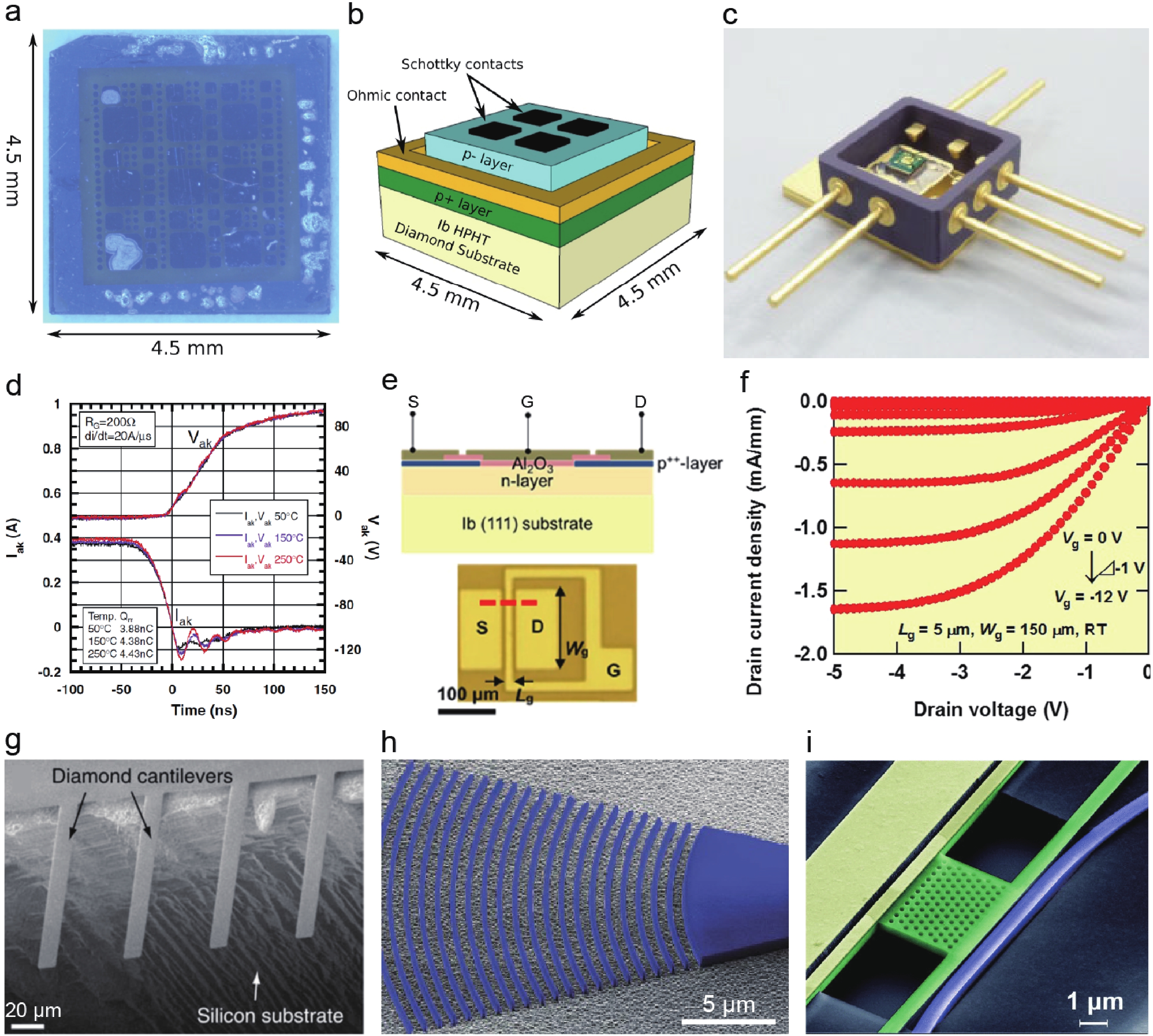
![(Color online) Representative diamond devices. (a, b) A picture and schematic of a diamond SBD[16]. (c) Diamond SBD is placed in a metal/ceramic container with high-temperature turn-off capabilities[24]. (d) Switching characterization of a diamond vertical SBD at 50, 150, and 250 °C, respectively[24]. (e) Schematic cross-section along with the red dot in a top-view optical picture of a MOSFET[31]. S, D, and G represent the source, drain, and gate contacts, respectively. (f) Drain current (Id) versus drain voltage (Vds) of a diamond MOSFET at room temperature[31]. (g) Scanning electron micrograph (SEM) of diamond-on-insulator devices with multiple cantilevers[40]. (h) SEM image of a fabricated compact focusing grating coupler device[41]. (i) SEM image of a freestanding diamond resonator in a fabricated electro-optomechanical device[42].](/richHtml/jos/2022/43/2/021801/img_1.jpg)
Fig. 1. (Color online) Representative diamond devices. (a, b) A picture and schematic of a diamond SBD[16 ]. (c) Diamond SBD is placed in a metal/ceramic container with high-temperature turn-off capabilities[24 ]. (d) Switching characterization of a diamond vertical SBD at 50, 150, and 250 °C, respectively[24 ]. (e) Schematic cross-section along with the red dot in a top-view optical picture of a MOSFET[31 ]. S, D, and G represent the source, drain, and gate contacts, respectively. (f) Drain current (I d) versus drain voltage (V ds) of a diamond MOSFET at room temperature[31 ]. (g) Scanning electron micrograph (SEM) of diamond-on-insulator devices with multiple cantilevers[40 ]. (h) SEM image of a fabricated compact focusing grating coupler device[41 ]. (i) SEM image of a freestanding diamond resonator in a fabricated electro-optomechanical device[42 ].
![(Color online) Synthetic diamonds. (a) Microwave plasma-assisted CVD growth of SCD over 70 large 3.5 × 3.5 mm2 HPHT seed crystals[11, 106]. (b) A mosaic wafer (40 × 40 mm2) in which CVD growth connects diamond plate fragments horizontally[77]. (c) A 155-carat freestanding pristine SCD with a thickness of 1.6 ± 0.25 mm and diameter of 90 mm fabricated by heteroepitaxy on Ir/YSZ/Si(001) in a microwave plasma CVD[76]. (d) An amorphous carbon material AM-III showing the intrinsic semiconducting nature with a bandgap of 1.5–2.2 eV[104].](/richHtml/jos/2022/43/2/021801/img_2.jpg)
Fig. 2. (Color online) Synthetic diamonds. (a) Microwave plasma-assisted CVD growth of SCD over 70 large 3.5 × 3.5 mm2 HPHT seed crystals[11 , 106 ]. (b) A mosaic wafer (40 × 40 mm2) in which CVD growth connects diamond plate fragments horizontally[77 ]. (c) A 155-carat freestanding pristine SCD with a thickness of 1.6 ± 0.25 mm and diameter of 90 mm fabricated by heteroepitaxy on Ir/YSZ/Si(001) in a microwave plasma CVD[76 ]. (d) An amorphous carbon material AM-III showing the intrinsic semiconducting nature with a bandgap of 1.5–2.2 eV[104 ].
Fig. 3. (Color online) Elastic strain engineering of diamond. (a–c) Schematic of the "push-to-bend" deformation of the nanoscale diamond needle with maximum deformation just before fracture, corresponding FEM simulation reproducing the geometry of the bending and displaying the local elastic maximum principal strain[148 ]. (d) "Compress-to-bend" deformation test on a FIB-machined single-crystalline nanoscale diamond needle along with [100] direction to the maximum bending deformation just before fracture and corresponding FEM simulation replicating the crucial nanoneedle shape and distribution of maximum principal strain[151 ]. (e, f) Uniaxial tensile setup of the diamond bridge with loading-full-unloading deformation, corresponding FEM simulation reproducing the geometry of the diamond bridge illustrating the longitudinal distribution of elastic strain[152 ]. (g) Tensile deformation of a diamond array with multiple bridges reaching a maximum tensile strain of 6%[152 ]. (h) Diamond bandgap envelope expanding to the semiconductor area with decreased bandgap. The black and red dots respectively denote the upper- and lower-envelope functions. The right side shows an illustration of bandgap isosurfaces in the ε 1ε 2ε 3 strain space[149 ]. (i) Detailed ε 11–ε 22 strain space showing an area of direct metal strains (brown) within the area of direct bandgap strains (blue) and an area of indirect metal strains (brown) within the nonzero indirect bandgap strains (white region with magenta symbols)[153 ]. (j) Three semiconducting, conducting, and superconducting stages of electronic bandgap evolution in progressively deformed diamond under (11
T c for a selected range of Coulomb pseudopotential μ *[154 ].

Set citation alerts for the article
Please enter your email address


