• Journal of Semiconductors
  • Vol. 43, Issue 2, 021801 (2022)
Chaoqun Dang1, Anliang Lu1, Heyi Wang1, Hongti Zhang2, and Yang Lu1、3、4
Author Affiliations
  • 1Department of Mechanical Engineering, City University of Hong Kong, Hong Kong, China
  • 2School of Physical Science and Technology, ShanghaiTech University, Shanghai 201210, China
  • 3Department of Materials Science and Engineering, City University of Hong Kong, Hong Kong, China
  • 4Nano-Manufacturing Laboratory (NML), Shenzhen Research Institute of City University of Hong Kong, Shenzhen 518057, China
  • show less
    DOI: 10.1088/1674-4926/43/2/021801 Cite this Article
    Chaoqun Dang, Anliang Lu, Heyi Wang, Hongti Zhang, Yang Lu. Diamond semiconductor and elastic strain engineering[J]. Journal of Semiconductors, 2022, 43(2): 021801 Copy Citation Text show less

    Abstract

    Diamond, as an ultra-wide bandgap semiconductor, has become a promising candidate for next-generation microelectronics and optoelectronics due to its numerous advantages over conventional semiconductors, including ultrahigh carrier mobility and thermal conductivity, low thermal expansion coefficient, and ultra-high breakdown voltage, etc. Despite these extraordinary properties, diamond also faces various challenges before being practically used in the semiconductor industry. This review begins with a brief summary of previous efforts to model and construct diamond-based high-voltage switching diodes, high-power/high-frequency field-effect transistors, MEMS/NEMS, and devices operating at high temperatures. Following that, we will discuss recent developments to address scalable diamond device applications, emphasizing the synthesis of large-area, high-quality CVD diamond films and difficulties in diamond doping. Lastly, we show potential solutions to modulate diamond’s electronic properties by the “elastic strain engineering” strategy, which sheds light on the future development of diamond-based electronics, photonics and quantum systems.

    1. Introduction

    Diamond has an extraordinary combination of outstanding characteristics, making it an 'extreme' material highly desirable for various applications. Due to its well-known mechanical properties, in particular hardness, it is extensively used as an abrasive and tooling material in a wide variety of industrial applications, including indenters, grinding, cutting, drilling, polishing, honing, sharpening, lapping, sanding, and wire drawing tools, usually in high-stress conditions. Additionally, they are responsible for the ability of diamond anvil cells with diamond compacts for high-pressure, high-temperature research[13] to apply materials to pressures found deep inside the Earth for various physical and geological studies. Besides these broad mechanical and structural applications, diamond serves as a road map for an unknown number of years in the development of power electronics and, more broadly, the whole microelectronics industry. Diamond semiconductors have attracted considerable interest in recent years[46] as a possible alternative for high-power high-frequency electronics in the next-generation integrated circuits due to the ultrawide bandgap[7, 8], ultra-high thermal conductivity[9], excellent dielectric breakdown field[5], long carrier lifetime, high saturation carrier velocity, and the highest electron and hole mobilities[10].

    Despite its outstanding features for electronics and photonic devices, considerable improvements are still anticipated since its present level is far lower. Its operation lifespan is far shorter than projected, and it has remained at the fundamental research level for decades. Additionally, reproducible and large-scale manufacture of diamond crystals continues to be a challenge[1113]. We shall begin this review by discussing the electronic characteristics of diamonds, which permit many electronic devices and nano- or micro-electromechanical systems. Then, we will discuss the present state of diamond wafer research and offer objectives for overcoming the present obstacles associated with synthesizing wafer-scale diamonds with low dislocation density and low resistivity. Finally, we shall cover alternative avenues for diamond electronics facilitation, particularly the so-called “elastic strain engineering” strategy based on microfabricated diamonds.

    2. Diamond electronic devices and nano- or micro-electromechanical systems

    Diamond is an enthralling semiconductor with extraordinary physical features, including ultrawide bandgap (5.47 eV), ultra-high thermal conductivity (2200 W/(m·K))[14], large breakdown electric field (10 MV/cm), high carrier saturation velocity (1.5–2.7 × 107 cm/s for electrons, 0.85–1.2 × 107 cm/s for holes)[5, 15] and high carrier mobility (4500 cm2/(V·s) for the electrons, 3800 cm2/(V·s) for the holes)[10]. Thanks to the combination of various extreme performances, diamond is an excellent platform for nano- and micro-fabrication, allowing for the development of a variety of robust sensors, diamond electronic devices, such as power diodes, switching devices, high-frequency field-effect transistors (FET), and nano- or micro-electromechanical systems (NEMS/MEMS), would perform exceedingly well.

    2.1. Diamond diodes

    The most often used semiconductor diode is a crystalline semiconductor material coupled to two electrical terminals through a p–n junction. For high-power and microwave switching, diodes serve as the basic structure, and they also serve as the building blocks for three-terminal devices. Both unipolar and bipolar diodes have been experimentally demonstrated, including p-type-intrinsic-n-type (p–i–n) diodes, Schottky barrier diode (SBD)[
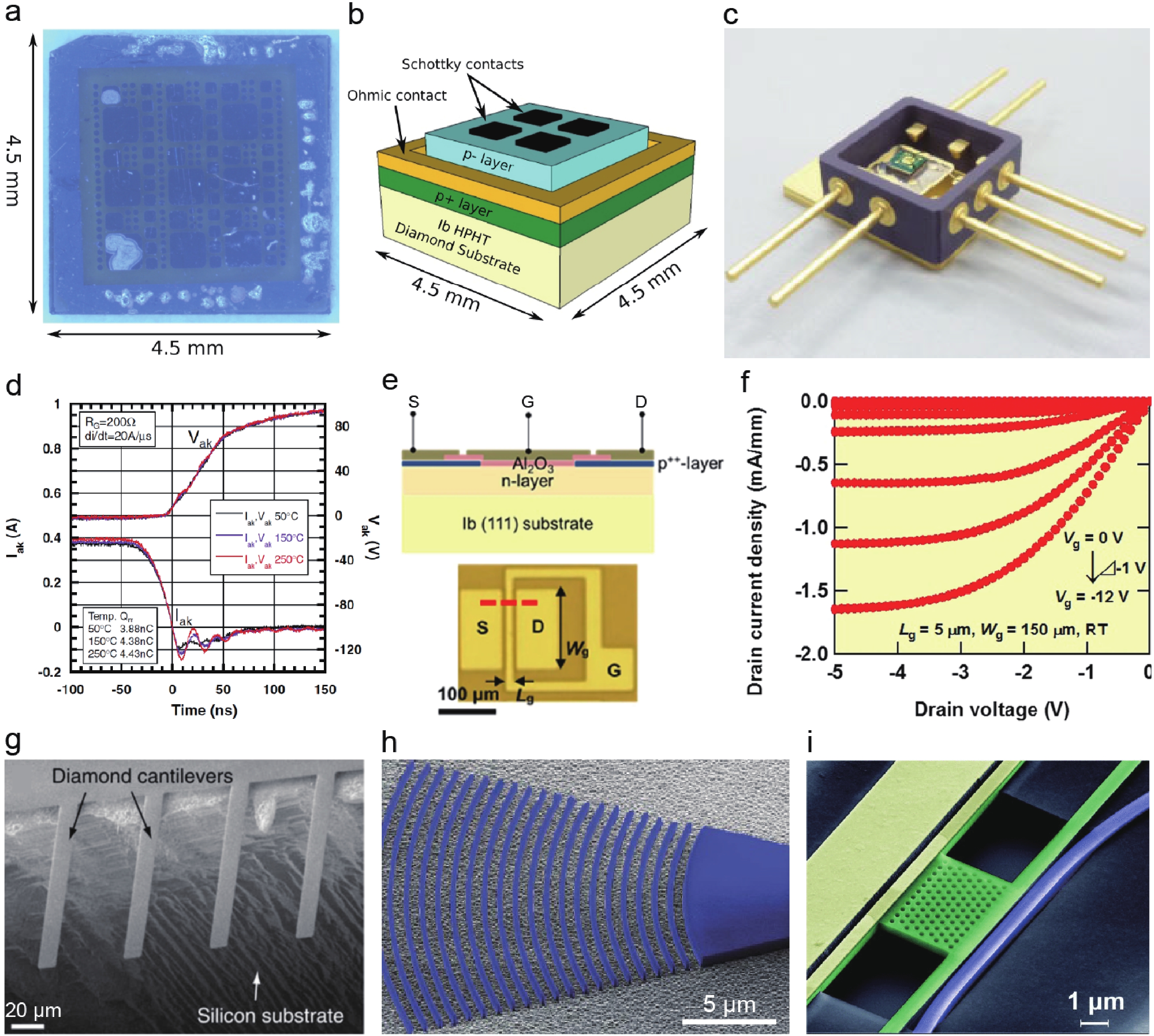
16] (Figs. 1(a) and 1(b)), junction barrier Schottky diodes (JBSDs), metal-intrinsic-p-type (M–i–P) diodes, and Schottky p–n diodes. One of the earliest diamond-based power devices was a high-temperature diode, composed of a Si-based Schottky material deposited on a homoepitaxial boron-doped diamond, which raised the working temperature of a Schottky diode structure above 1000 °C[3]. Numerous studies have revealed details about the construction of an M–i–P diode[1719]. The M–i–P Schottky barrier diode configuration can compensate for the absence of carriers in the drift zone and can resist breakdown voltages of a few kilovolts with thin drift regions (< 25μm) due to the diamond’s high critical field strength. A breakdown voltage of up to 10 kV with a corresponding electric field of 7.7 MV/cm was found for a p–i–n diode[20], which could be a cutting-edge and attractive diamond device for high-power applications. Although the electrical properties of diamond p–i–n diodes under static conditions have been widely studied, the switching characteristics are still unclear, and the recovery waveform is the primary concern. Traoré et al.[21] studied the switching capabilities for diamond p–i–n diodes when they were utilized as freewheeling diodes. It can be switched from the on-state to the blocking state at 850 A/cm2, and the time required for reverse recovery is 150 ns. In addition, Schottky barrier diodes with a high-power figure of merit (244 MW/cm2)[22], and forward direct-current (DC) current (20 A)[23], as well as fast operation with low-loss switching[24] (Figs. 1(c) and 1(d)) have also been successfully fabricated. Shimaoka et al.[25] demonstrated a betavoltaic cell with a super-efficient conversion, approaching the theoretical limit of Shockley–Queisser efficiency, utilizing a diamond p–n junction. Perez et al.[16] demonstrate that diamond devices may substantially enhance the capability of power converters, particularly at elevated temperatures. At 450 K junction temperature, diamond semiconductors may reduce semiconductor losses and heatsink volume three times compared to SiC devices. Additionally, they show that switching frequencies in diamond-based power converters may be five times greater than in SiC-based power converters, with lower overall semiconductor losses and a smaller heatsink.

    (Color online) Representative diamond devices. (a, b) A picture and schematic of a diamond SBD[16]. (c) Diamond SBD is placed in a metal/ceramic container with high-temperature turn-off capabilities[24]. (d) Switching characterization of a diamond vertical SBD at 50, 150, and 250 °C, respectively[24]. (e) Schematic cross-section along with the red dot in a top-view optical picture of a MOSFET[31]. S, D, and G represent the source, drain, and gate contacts, respectively. (f) Drain current (Id) versus drain voltage (Vds) of a diamond MOSFET at room temperature[31]. (g) Scanning electron micrograph (SEM) of diamond-on-insulator devices with multiple cantilevers[40]. (h) SEM image of a fabricated compact focusing grating coupler device[41]. (i) SEM image of a freestanding diamond resonator in a fabricated electro-optomechanical device[42].

    Figure 1.(Color online) Representative diamond devices. (a, b) A picture and schematic of a diamond SBD[16]. (c) Diamond SBD is placed in a metal/ceramic container with high-temperature turn-off capabilities[24]. (d) Switching characterization of a diamond vertical SBD at 50, 150, and 250 °C, respectively[24]. (e) Schematic cross-section along with the red dot in a top-view optical picture of a MOSFET[31]. S, D, and G represent the source, drain, and gate contacts, respectively. (f) Drain current (Id) versus drain voltage (Vds) of a diamond MOSFET at room temperature[31]. (g) Scanning electron micrograph (SEM) of diamond-on-insulator devices with multiple cantilevers[40]. (h) SEM image of a fabricated compact focusing grating coupler device[41]. (i) SEM image of a freestanding diamond resonator in a fabricated electro-optomechanical device[42].

    2.2. Field-effect transistors

    Diamond has been investigated in the exploitation of prototype field-effect transistors (FETs). At the moment, several designs for power electronics applications which is suitable to high temperature and radiation settings are being investigated. Lee et al.[26] reported a hydrogen-terminated diamond (H-diamond, a common way using to increase the diamond’s surface conductivity[2729]) transistor that demonstrates a favorable symbiosis of metal-insulator-semiconductor FET (with ON and OFF current of 0.8 and 10–9μA/μm, respectively) and metal–semiconductor FET with near-perfect subthreshold (swing of 67 mV/dec) performance operations in the same single multilayered device. Zhang et al.[30] demonstrated a drain-source voltage of –20 V and a current on-off ratio over 109 for Y/Al2O3/H-terminated diamond FET, which meet the practical standard. Diamond-based power metal–oxide–semiconductor FETs (MOSFETs) have also been shown in recent years. Matsumoto et al.[31] developed diamond MOSFETs with an inversion channel and typically off properties using phosphorus-doped n-type matrix on a (111) diamond and atomic layer deposition Al2O3 gate oxide. Its schematic cross-section and top-view image are shown in Fig. 1(e). The negative gate voltage regulated the drain current, forming an inversion channel with a p-type feature at the interface between the n-type diamond and the Al2O3 layer. As shown in Fig. 1(f), the diamond MOSFET shows the highest drain current density of 1.6 mA/mm and field-effect mobility of 8.0 cm2/(V·s) at room temperature. Recently, the concept of a deep-depletion diamond MOSFET is developed and proven to be an excellent choice for developing competent diamond MOSFETs[32]. Masante et al.[33] demonstrated a bidirectional diamond deep-depletion MOSFET with 250 °C operations quasi-static characteristics, a threshold voltage of about 35 V, and a low minimum gate leakage current of 1.00 × 10⁻⁴ mA/mm at a gate–source bias VGS = 50 V, which is promising when used at high voltage and high temperature.

    2.3. Diamond nano- or micro-electromechanical systems

    NEMS/MEMS have attracted interest in various applications, including accelerometers, physical, biological, and chemical sensors. Diamond has demonstrated itself as an ideal candidate for developing robust, high-reliable, and long-endurance NEMS/MEMS in harsh environments due to its excellent physical, chemical, electrical, and tribomechanical characteristics[3439]. Great effort and progress have been made in developing diverse diamond NEMS/MEMS structures among single-crystalline, polycrystalline, nanocrystalline, and ultra-nanocrystalline diamonds. Micro- or nanoscale mechanical resonators bring exciting perspectives for ultrasensitive sensing, precise measurements, and quantum technologies. As quantum mechanical device elements, diamond resonators linked to optical cavities or spins have been extensively investigated for quantum science and technology. For instance, Tao et al.[40] manufactured single-crystalline diamond (SCD) cantilevers with a thickness of 85 nm and lateral length of up to 240 μm (Fig. 1(g)). They demonstrated their ultrahigh quality factors over one million at room temperature, which exceeds those of state-of-the-art single-crystalline silicon cantilevers with a comparable size by nearly an order of magnitude. Besides, full-scale optomechanical circuits were fabricated in wafer-scale polycrystalline diamond thin film substrates[41]. The utilization of freestanding diamond nano-mechanical resonators demonstrated the efficient optomechanical transduction through optical gradient forces (Fig. 1(h)) with quality factors of over 11 200 integrated into on-chip Mach-Zehnder interferometers. Rathet al.[42] show active modulation of diamond nano-photonic circuits by utilizing mechanical flexibility in freestanding diamond electro-optomechanical resonators (Fig. 1(i)) with high-quality factors over 9600.

    Additionally, theoretical proposals and fundamental experiments to mechanically couple NEMS/MEMS devices to intrinsic quantum two-level systems can be achieved in a diamond nano-mechanical resonator of embedded nitrogen-vacancy (NV) centers[4345]. Wilson-Rae et al.[44] demonstrated that a diamond nano-mechanical resonator mode could be cooled to its ground state. Moreover, Barfusset al.[46] incorporated a single electronic spin into an integrated quantum device. They produced long-lived, coherent oscillations of an embedded NV center spin and extended the NV’s spin coherence duration by introducing the time-varying strain in a diamond cantilever. Riedrich-Moller et al.[47] proposed a way to manufacture 1D and 2D photonic crystal microcavities in a single-crystalline diamond. They found the cavity modes can be modulated resonance with the zero-phonon line with an increased intensity factor of 2.8. This controlled coupling of color centers to photonic crystal microcavities may open possibilities for larger-scale diamond photonic quantum devices.

    2.4. Microfabrication techniques of diamond devices

    Fabrication of diamond devices and NEMS/MEMS is often challenging, in particular for single-crystalline diamond (SCD), since they can only be from homoepitaxially/heteroepitaxial growth on previously grown SCD or other substrates. As a result, the accessible SCD templates are just a few tens of millimeters square. Manufacturing diamond devices and NEMS/MEMS typically begins with the fabrication of a diamond thin film or membrane, which is then followed by the assembly of the devices. Methods have been investigated that include the “thin down” technique, the liftoff method, the angle-etching procedure, and focused ion beam milling[48, 49].

    The “thin down” technique begins with a bulk diamond with a thickness of tens of microns. It is subsequently thinned down to a thickness of a few hundred nanometers through dry etching by capacitively coupled reactive ion etching (RIE)[50]. This technique is frequently limited in size or susceptible to thickness variations in the bulk slab, demanding additional safeguards[51]. Following that, structures are patterned using electron beam lithography (EBL) and dry etching. The liftoff method by ion implantation may eliminate the thickness fluctuations[5254]. The ion-implanted diamond produces a damaged layer, which will transform to an etchable carbon layer after the annealing process and can be removed selectively using wet etching. EBL and dry etching can shape the structures after reproducing a new diamond layer, eliminating any damaged diamond layers, and transferring the new diamond layer to a new substrate. In the angle etching method[55, 56], the diamond is first printed with an etch mask, then etched top-down on a rotating sample stage perpendicular to the ion beam direction. After achieving the required vertical depth, the sample is tilted to the collimated ion beam at an acute angle. Angled etching involves rotating the sample stage to etch beneath the mask, and the etch mask is removed after the required undercut has been achieved. This technique enables the direct construction of freestanding devices in the bulk diamond without the requirement for prior thin-down. Still, it limits the design flexibility since the etching angle automatically fixes the height of the resultant structure for a given device width. Focused ion beam (FIB) milling is the most controllable technique[47, 53, 57] that usually utilizes Ga or other ions to directly produce electron-transparent membranes with sub-micron positional precision. This technique enables the direct patterning of diamonds without the requirement for a mask, but is often costly. Still, it has certain disadvantages in potential structural damage, implanted ions, and process scalability[53, 5861], which may be overcome by being coupled with electron-beam-induced etching and other processes in the future.

    3. Challenges on scalable diamond devices

    For mass production of industrial semiconductor devices, semiconductor materials are required to achieve high purity, low defect density, high carrier concentration and mobility, and large area wafer. However, doping and fabrication of high-quality large-area SCD wafers are still worldwide scientific problems for diamond materials. The tremendous potential for realizing diamond devices above present device technology is contingent upon achieving several key objectives, including the synthesis of ultrahigh purity, high-quality wafer-scale SCDs, and the ability to provide carriers via controlled doping.

    3.1. Growth of large-area single-crystalline diamond wafers

    Although commercially accessible high-quality polycrystalline diamond has many attributes comparable to the finest natural diamonds, grain boundaries can still impact its electronic performances due to the crystal defect nature and existence of various impurities such as nitrogen, silicon, and others[62]. The polycrystalline diamond devices prohibit them from achieving the maximum performance predicted by SCD characteristics in numerous applications. As a result, electronic devices have significantly reduced charge carrier mobility[26], and detectors experience insufficient charge collection[27], leaving SCD to be the only alternative for the most demanding applications.

    For the past 70 years, synthetic SCDs have been manufactured using high-pressure, high-temperature (HPHT) processes[6366] and, recently, chemical vapor deposition (CVD) technology[6769]. Although SCDs generated through the HPHT process have an extraordinarily low dislocation density[70, 71], doping is difficult to manage. Furthermore, since the growing device intrinsically constrains the diameter of the HPHT diamond, it is inappropriate for wafer manufacture and very large-scale integration (VLSI). The CVD method enables the production of diamonds with a high degree of crystallinity under precisely regulated circumstances, substantially lower nitrogen content with a few hundred parts per million[72], and can better control the incorporation of impurities by adjusting the growth chemical process. Additionally, CVD growth can provide high-quality large-size SCDs suitable for diamond photoelectric applications.

    Numerous approaches to large-area SCD wafer (Figs. 2(a)–2(c)) synthesis reach 50 mm in diameter. In homoepitaxy, single crystals, such as those obtained by the HPHT method, are utilized as seeds and are replicated namely "mosaic" wafer. Among the numerous techniques for CVD diamond, microwave plasma CVD has attracted significant attention owing to its ability to combine high purity with rapid growth rates (>100μm/h)[73] and sufficient lateral dimensions (6 inches)[74]. For example, microwave plasma CVD was used to fabricate mosaic diamonds wafer 2 inches (40 × 60 mm2)[75] or above[69, 76] in size via the lateral tiling of smaller SCD plates made using a smart-cut-like extraction technique from tiny HPHT produced boules. In the lateral tiling growth, an ensemble of identically oriented clones is positioned next to one another, and their lateral dimensions may be somewhat enlarged under appropriate growing circumstances. However, one of the primary problems concerning such wafers' applicability is internal coalescence boundaries, as shown in Fig. 2(b)[77]. Due to the loss in device consistency, such extremely imperfect structures diminish the electrical performance.

    (Color online) Synthetic diamonds. (a) Microwave plasma-assisted CVD growth of SCD over 70 large 3.5 × 3.5 mm2 HPHT seed crystals[11, 106]. (b) A mosaic wafer (40 × 40 mm2) in which CVD growth connects diamond plate fragments horizontally[77]. (c) A 155-carat freestanding pristine SCD with a thickness of 1.6 ± 0.25 mm and diameter of 90 mm fabricated by heteroepitaxy on Ir/YSZ/Si(001) in a microwave plasma CVD[76]. (d) An amorphous carbon material AM-III showing the intrinsic semiconducting nature with a bandgap of 1.5–2.2 eV[104].

    Figure 2.(Color online) Synthetic diamonds. (a) Microwave plasma-assisted CVD growth of SCD over 70 large 3.5 × 3.5 mm2 HPHT seed crystals[11, 106]. (b) A mosaic wafer (40 × 40 mm2) in which CVD growth connects diamond plate fragments horizontally[77]. (c) A 155-carat freestanding pristine SCD with a thickness of 1.6 ± 0.25 mm and diameter of 90 mm fabricated by heteroepitaxy on Ir/YSZ/Si(001) in a microwave plasma CVD[76]. (d) An amorphous carbon material AM-III showing the intrinsic semiconducting nature with a bandgap of 1.5–2.2 eV[104].

    In heteroepitaxy, the substrate is critical for the SCD's properties: easy acquisition of high-quality and large-size substrates, the substrate's lattice mismatch with diamond to reduce misfit dislocations at the interface, excellent thermal expansion coefficient matching with diamond to reduce thermal stress, carbon's solubility in the substrate, and the interaction with C atoms (specifically, its inclination to produce stable carbides) all affect the nucleation and growth of diamond. c-BN[78, 79], Pt[80], Ni[81], Co[82], Ir, Si[83], SiC[84], TiC[85] are all common substrates for the growth of SCDs. At present, investigations[76, 86, 87] conducted over several decades have shown that Ir is the most promising substrate for heteroepitaxy growth of diamonds. Additionally, numerous studies have been conducted to ascertain the physical explanations underlying its uniqueness[8892]. Essentially, a range of alternate substrate materials (Si, Cu, Ni, Re, β-SiC, TiC) enables the formation of the specific oriented diamond. The density of epitaxial diamond grains on all alternative substrates was much lower than Ir, and their orientation dispersion was substantially larger. Therefore, even elongated growth could not form true single crystals from epitaxial layers.

    Nevertheless, due to the scarcity of single-crystalline Ir substrates, Ir multilayer substrates (such as Ir/MgO[93, 94], Ir/sapphire[9597], Ir/STO (strontium titanate)/Si[98, 99], Ir/YSZ (yttria-stabilized zirconia)/Si[76, 100,101]) have been proved to be the extraordinary candidates for diamond nucleation and growth with a structural quality unrivaled by any other (scalable) substrate[102]. However, the coefficients of thermal expansion MgO, SrTiO3, and even sapphire still significantly diverge from that of diamond, which results in enormous thermal stress in the Ir multilayer after being cooled[103]. In comparison to these substrates, silicon is by far proved to be the best choice[103]. The growth of diamond on Ir/SrTiO3/Si substrate shows a homogeneous and dense structure with good crystalline quality by the bias enhanced nucleation technique[98, 99]. Schreck et al.[76] have reached the stage where heteroepitaxial diamond with a diameter of 92 mm can be achieved by the introduction of the multilayer substrate Ir/YSZ/Si (100), as shown in Fig. 2(c). Recently, an amorphous diamond-like carbon material[104] with a high percentage of sp3 bonding was synthesized and demonstrated to be the hardest and strongest amorphous material known to date, capable of scratching natural diamond, as shown in Fig. 2(d). Besides its remarkable mechanical characteristics, it may also be utilized in electronics and photovoltaic applications due to its semiconducting nature with a bandgap of 1.5–2.2 eV. Moreover, they further fabricated a semiconducting amorphous carbon with a narrow bandgap of 0.1–0.3 eV from fullerene C60 powder, exhibiting isotropic super hardness and superior toughness[105].

    3.2. Doping of diamond

    Several issues should be fixed to fully use diamond's electrical capabilities before this material can be used largely. The primary impediment[107109] is achieving an effective n-and p-type doped diamond that could be utilized to fabricate a bipolar electronic device's essential building block – the p–n junction. Owing to the large bandgap of 5.47 eV, pure diamond is a superb insulator. At room temperature, its inherent carrier concentration is very low, and as a result, the resistivity of pure diamond may surpass 1016 Ω·cm[110]. Over past decades, researchers have sought to exploit diamond's extremely desired characteristics for various electrical device applications. As is the case with the bulk of today's semiconducting materials, diamond's crystal lattice must be doped to get suitably stable, mobile, and high-density charge carriers. Efforts to develop a mature diamond doping technique have met several challenges. The ionization energy of dopants in wide bandgap (WBG) semiconductors is greater than that in narrow bandgap semiconductors, leading to a low activation temperature. For instance, 4-H SiC possesses shallow donors (n-dopant) but no shallow acceptors (p-dopant). Known dopants have much higher ionization energy in the diamond; obtaining shallow donors and deep acceptors in diamond using impurity doping with activation energies adequate for room temperature operation is incredibly challenging, as in other WBGs.

    3.2.1. p-type diamond

    Boron, one less electron than carbon, is very easy to integrate into diamond due to its tiny atomic radius[111]. Since boron functions as a charge acceptor, the resultant diamond is essentially hole-doped. Boron-doped p-type diamonds occur naturally. Boron established itself as one of the most hopeful impurity donors for p-type doping in diamond, despite its relatively high activation energy of 0.37 eV[8, 112]. It has been the 'dopant of choice' since the 1970s. CVD methods have been used to fabricate boron-doped diamonds by mixing B-containing molecules in either a microwave (MW) or a hot filament (HF) reactor, leading to the formation of boron-doped p-type diamond. Teukam et al.[113] realized a high-conductivity n-type diamond through the deuteration of homoepitaxially synthesized boron-doped (100) diamond films with electrical conductivities up to 2 Ω–1cm–1 and electron mobilities of a few hundred cm2/(V·s) at room temperature. Furthermore, Ekimov et al.[114] experimentally found superconductivity in near 3% boron-doped diamond with a superconducting transition temperature of Tc ≈ 4 K. Its superconductivity sustains in magnetic fields up to Hc2(0) ≥3.5 T. Then, theoretical work indicated an electron-phonon coupling mechanism[115120]. Kawano et al.[121] investigated the critical boron doping content (9 × 1020 cm–3) of the superconductivity of (110) diamond film, which is higher than 3 × 1020 cm–3 of the (111) and (001) diamond films owing to the presence of boron atoms in the interstitial space. Lloret et al.[122] proposed a method for growing homoepitaxial diamonds specifically doped with boron for diamond electrical devices by a microwave plasma-enhanced CVD method. The boron-doped p-type diamond is already well-established and commercially available. However, the mobility of holes in boron-doped diamond has been found to be reduced substantially when either the dopant concentration or the temperature rises[10, 123125], which hinders its high-temperature applications.

    3.2.2. n-type diamond

    On the other hand, n-type diamond does not occur naturally, and it is challenging to acquire n-type semiconducting diamond with high quality. Since the early 1980s, when the CVD method for the growth of diamond was developed, n-type doping has been studied. Based on the conventional dopants used in Si, it is anticipated that group V (N, P) and VI (S) elements in diamond are promising donor impurities. Nitrogen (with its extra electron compared to C) is the most common impurity in an n-type diamond. Nitrogen exists in diamonds in alternative ways, and substitutional nitrogen easily enters the diamond lattice, which fits in with its negative formation energy (–3.4 eV)[126]. However, it is an extremely deep donor level with approximately 1.7 eV below the conduction band in the diamond, which maintains the insulative of the diamond at room temperature. Despite the high activation energy of 0.6 eV for phosphorous at ambient temperature, it remains the most popular donor for n-type impurity doping of diamond[127131]. Yuet al.[132] fabricated a phosphorus-doped diamond via the CVD growth method and used it as the electrode to fabricate supercapacitors. Koizumi et al.[129] studied the semiconducting characteristics of phosphorus-doped diamond films deposited by a metal-chamber-type microwave plasma-assisted CVD method across a broad temperature range using Hall measurements. At room temperature, the n-type conductive diamond film achieved on a (111)-oriented diamond substrate exhibits mobility up to 100–240 cm2/(V·s). The carrier's activation energy was approximately 0.6 eV. Kato et al.[133] fabricated a phosphorus-doped n-type (001)-oriented SCD using homoepitaxial growth plasma-enhanced method through introducing PH3 gas. The n-type conductive diamond showed the highest mobilities of about 350 cm2/(V·s) by Hall-effect measurements.

    The poor phosphorus incorporation efficiency is still a serious obstacle, although Ohtani et al.[134] reported a method to increase the doping efficiency by systematically changing the internal design of the CVD chamber. Moreover, although phosphorus-doped diamond film achieved donor concentrations up to 6.8 × 1016 cm–3, the activation energy was so high that the carrier concentration was restricted to 1011 cm–3 at room temperature[129]. Sakaguchiet al.[135] successfully achieved sulfur-doped homoepitaxial (100)-oriented diamond film. They confirmed that it showed n-type conduction through Hall-effect measurements in the temperature from 250 to 550 K. The film showed 597 cm2/(V·s) electron mobility at room temperature. The ionization energy was 0.38 eV. However, Kalish et al.[136] demonstrated that the Hall coefficient of sulfur-doped diamond was consistently positive, indicating p-type conductivity as a function of temperature, with activation energies, carrier concentrations, and mobilities that are extremely similar to those of boron-doped p-type diamond, which indicated that which was formerly assumed to be n-type owing to a donor state ascribed to sulfur, containing sufficient accidental boron to account for the observed p-type characteristics. It should, however, be noted that calculations[137] do not exclude the likelihood that sulfur in diamond exhibits donor-related conductivity, which is especially apparent at elevated temperatures.

    4. Elastic strain engineering of diamond

    Elastic strain engineering (ESE) can bring materials with unique characteristics by applying considerable mechanical stress or strain[138]. In fact, “strain engineering” has been a commonly utilized technique for optimizing the performance of semiconductor devices. For example, stress may increase a semiconductor's electron mobility, allowing more efficient solar cells[139] and smaller, quicker transistors[140]. Now, as the development of "ultra-strength"[141, 142] materials, referring to a material reaching sample-wide stress exceeding a substantial percentage (>1/10) of its theoretical strength over a prolonged length of time, mechanical straining has been an effective approach to modulate semiconductors at small length scales due to well-known “size effect”, that is, “smaller is stronger”. At the nanoscale, even "deep ultra-strength"[143], referred to the sample-wide stress reaching one half of the bulk theoretical strength, can be achieved and applied for deep strain engineering of functional devices. Deep ESE thus defines the elastic strain as going beyond half of its theoretical strain. Previous density functional theory calculations[99102] found that the bandgap structure of diamond under large strains will undergo fundamental changes, which could open up new avenues for diamond electronics. However, due to bulk diamonds' extremely high hardness and brittleness, the deep ESE strategy for diamonds has long been regarded as infeasible. This part will review the recent efforts to realize the diamond's elastic deformation and deep elastic strain engineering.

    4.1. Elastic deformation of diamond

    In past decades, the mechanical properties of diamond have been investigated using various techniques such as indentation[144], scratch[145], and diamond anvil cell compression[146]. However, these tests produced complicated stress states, and the elastic strain was generally limited (<1%). In recent years, with the advancement of micro/nano-mechanical testing technologies and nano-manufacturing, it has been possible to conduct micro/nano-mechanical tests on diamond. Wheeleret al.[147] performed the uniaxial compressive test of the focused ion beam (FIB)-machined diamond pillars and, for the first time, experimentally realized the theoretical limits of strength. Then, Banerjeeet al.[148] discovered that single-crystalline diamond needles at the nanometer scale have unexpectedly high elasticity and can locally produce large elastic deformation up to 9% by a unique "push-to-bend" testing strategy, as shown in Figs. 3(a)–3(c)[148]. This discovery reveals the possibility of modulating the physical properties of the diamond through a whole new strategy, i.e., deep ESE[149, 150]. Moreover, Nie et al.[151] demonstrated the maximum tensile strain and strength that can be achieved of single-crystalline diamond nanoneedles along with [100], [110], and [111] directions with various diameters by the similar "compress-to-bend" method. They further achieved up to 13.4 % elastic strain of [100]-oriented diamond, which approaches its theoretical strain limits (Fig. 3(d)). However, accuracy control at a sufficiently massive volume is required to fully exploit deep ESE in real device applications. Efforts to stretch diamonds were often restricted by the strain contained inside a limited sample volume due to flexural bending, producing an uneven strain distribution. These specimens were also difficult to manage, and the resultant area/volume under large strains is extremely concentrated.

    (Color online) Elastic strain engineering of diamond. (a–c) Schematic of the "push-to-bend" deformation of the nanoscale diamond needle with maximum deformation just before fracture, corresponding FEM simulation reproducing the geometry of the bending and displaying the local elastic maximum principal strain[148]. (d) "Compress-to-bend" deformation test on a FIB-machined single-crystalline nanoscale diamond needle along with [100] direction to the maximum bending deformation just before fracture and corresponding FEM simulation replicating the crucial nanoneedle shape and distribution of maximum principal strain[151]. (e, f) Uniaxial tensile setup of the diamond bridge with loading-full-unloading deformation, corresponding FEM simulation reproducing the geometry of the diamond bridge illustrating the longitudinal distribution of elastic strain[152]. (g) Tensile deformation of a diamond array with multiple bridges reaching a maximum tensile strain of 6%[152]. (h) Diamond bandgap envelope expanding to the semiconductor area with decreased bandgap. The black and red dots respectively denote the upper- and lower-envelope functions. The right side shows an illustration of bandgap isosurfaces in the ε1ε2ε3 strain space[149]. (i) Detailed ε11–ε22 strain space showing an area of direct metal strains (brown) within the area of direct bandgap strains (blue) and an area of indirect metal strains (brown) within the nonzero indirect bandgap strains (white region with magenta symbols)[153]. (j) Three semiconducting, conducting, and superconducting stages of electronic bandgap evolution in progressively deformed diamond under (11)[111] compression-shear strain and strain dependence of critical temperature Tc for a selected range of Coulomb pseudopotential μ*[154].

    Figure 3.(Color online) Elastic strain engineering of diamond. (a–c) Schematic of the "push-to-bend" deformation of the nanoscale diamond needle with maximum deformation just before fracture, corresponding FEM simulation reproducing the geometry of the bending and displaying the local elastic maximum principal strain[148]. (d) "Compress-to-bend" deformation test on a FIB-machined single-crystalline nanoscale diamond needle along with [100] direction to the maximum bending deformation just before fracture and corresponding FEM simulation replicating the crucial nanoneedle shape and distribution of maximum principal strain[151]. (e, f) Uniaxial tensile setup of the diamond bridge with loading-full-unloading deformation, corresponding FEM simulation reproducing the geometry of the diamond bridge illustrating the longitudinal distribution of elastic strain[152]. (g) Tensile deformation of a diamond array with multiple bridges reaching a maximum tensile strain of 6%[152]. (h) Diamond bandgap envelope expanding to the semiconductor area with decreased bandgap. The black and red dots respectively denote the upper- and lower-envelope functions. The right side shows an illustration of bandgap isosurfaces in the ε1ε2ε3 strain space[149]. (i) Detailed ε11ε22 strain space showing an area of direct metal strains (brown) within the area of direct bandgap strains (blue) and an area of indirect metal strains (brown) within the nonzero indirect bandgap strains (white region with magenta symbols)[153]. (j) Three semiconducting, conducting, and superconducting stages of electronic bandgap evolution in progressively deformed diamond under (11 )[111] compression-shear strain and strain dependence of critical temperature Tc for a selected range of Coulomb pseudopotential μ*[154].

    4.2. Uniform tensile elastic straining of diamond

    With the improved microfabrication techniques, as shown in Fig. 3(e), single-crystalline diamond bridge structures can be precisely microfabricated by FIB-assist processes, and a uniaxial tensile test can be realized for such smooth diamond specimens by using a nanoindenter with a customized tensile diamond gripper[105]. Such diamond microbridges exhibited a significantly uniform, large elastic deformation of approximately 7.5% strain through the entire gauge area of the bridge during quantitative tensile testing, rather than deforming in a limited region during bending, as shown in Fig. 3(f). Ultralarge uniform elastic strains (6%–8%) in microfabricated diamonds orientated in the [100], [101], and [111] directions were consistently achieved. Up to 9.7% uniform tensile strain was then realized by refining the sample shape by adopting the American Society for Testing and Materials (ASTM) standard for brittle tensile specimens, which approaches the diamond's theoretical elastic limit. Besides, in situ straining of the microfabricated diamond array containing multiple bridges was also realized, indicating a large, uniform, and reversible straining among the multiple diamond bridges to demonstrate diamond-based ESE device applications, as shown inFig. 3(g). These discoveries pave the way for practical applications and provide fundamental solutions for applying deep elastic strain engineering of diamond devices, which opens the wide application potential of "strained diamond" in electronics and optoelectronics.

    4.3. Tuning electronic properties of strained diamonds

    The experimental discoveries have established that the diamond can be elastically deformed up to its theoretical strain limits. These advances offer possibilities to explore its functional performances by elastic strain engineering. A surprising atomistic ductility and electronic conductivity were revealed in diamonds under complex loading conditions of large concurrent shear and compressive strains by density functional theory (DFT) calculation[150]. The electronic bandgap of diamond decreased with increasing pure shear strain and constrained shear strain, the opposite to the increase of bandgap with homogeneous compressive strain. Then, Shi et al.[149] studied the effects of full six-dimensional space of admissible nonlinear elastic strain on the bandgap of the diamond by high-accuracy machine learning methods. They found that finding the most energy-efficient strain paths could convert diamond from an ultrawide bandgap material to a wide-bandgap semiconductor comparable to InAs, as shown in Fig. 3(h). Moreover, Dang et al.[152] show the relationship between uniaxial strain and calculated bandgap values along with [100], [101], and [111] directions according to corresponding experimental results. The bandgap values were found to be a decreasing trend for three directions as the strain increased, and an indirect-to-direct transition may achieve along with the [111] direction with applied strain over 9%. Experimental characterization of the bandgap was conducted on a bent T-shaped sample by electron energy loss spectroscopy (EELS), which verified the decreasing trend by calculation. Furthermore, the diamond may undergo reversible metallization, demetallization, and indirect-to-direct bandgap transitions, if the strain levels required for phonon instability are kept below the threshold values (Fig. 3(i))[153]. Liu et al.[154] discovered an unexpected path to superconductivity in diamond via compression shear deformation. As the strain increases, increasing metallization and lattice softening occur, resulting in phonon mediated critical temperature Tc ranging from 2.4 to 12.4 K for a wide range of Coulomb pseudopotential μ* = 0.15–0.05 (Fig. 3(j))[154].

    5. Conclusions and perspectives

    With the increasing need for wide bandgap semiconductors, the arrival of 5G and even future 6G networks, and the demand for power electronics chips for electric vehicles, diamond has become an ideal electronic material for such critical applications. Here, we can only briefly cover a few efforts on diamond-based high voltage switching diodes, high-power high-frequency FET, devices operating at high temperatures, and MEMS/NEMS. Although diamond offers enormous potential, it also has several characteristics that pose difficulties. We then described the production issues, including the wafer-scale production of electronics-grade high-quality diamonds. Significant progress has been made on high-quality CVD diamond thin films with a 4-inch diameter[76] or larger, but defects still have to be minimized. The dimension of the homoepitaxial diamond is also increasing, particularly when the mosaic technique is used[69, 75, 76]. We believe the high-efficiency manufacturing of the large-area high-quality diamond wafer can be realized by developing advanced equipment and improving homoepitaxial and heteroepitaxial growth techniques in the near future. The increasing SCDs sizes would promote the production of diamond-based electronic devices in the future, where point defects are not as detrimental as they are in electrical devices.

    We also described the shallow doping problems in diamonds for realizing diamond microelectronics applications. The growth and application of p-type diamonds with boron-doping are considerably mature. Ion implantation or CVD may be used to precisely control the impurity level and carrier transport performance. The absence of effective and practical n-type conductive diamond materials, on the other hand, restricts the use of diamond semiconductor materials in the electronic field. In general, there are still great difficulties in the synthesis of low-resistivity n-type diamond films. It deserves further investigation into improving doping technology, increasing electron mobility, and reducing resistivity in the fabrication of n-type diamond semiconductors. We then proposed an alternative way, “elastic strain engineering”, to modulate a diamond’s electronic properties, which was considered impossible due to its inherent mechanical characteristics. Now with the development of microfabrication techniques, ultralarge elastic strains can be well realized in diamond micro/nanostructures[148, 151, 152] through the size effect, and the bandgap values of the diamond can be then tuned by elastic straining, as further suggested by some advanced simulations[149, 150], which make it possible for elastic strain engineering of diamond under complicated load configurations. Theoretically, it is even possible to achieve metallization[153] in the diamond when imposing extreme strain values, or even superconducting state by combining compression-shear deformations[154], which may open infinite possibilities in the future development of diamond electronic devices.

    Additionally, as diamond is also a popular quantum material[155, 156], it is found that diamond single quantum systems can also be controlled by imposing mechanical strain, in contrast to established methods that rely on electromagnetic fields. Strain, for example, has already been suggested to be utilized to transport information between remote quantum systems[157] and cool mechanical oscillators to their quantum ground state[44], which opens new perspectives for quantum information technologies.

    Nevertheless, grand challenges remain in permitting diamond microelectronics and optoelectronics to the industry level. For example, establishing the planar processing of diamond for high-efficiency and reproducible large-scale manufacturing would be the primary challenge for building individual components of integrated circuit chips. Besides, maintaining the robust, highly strained diamond for an extended length of time with accurate bandgap control and characterization would be another challenge. A lattice mismatch of diamond films grown on different heterogeneous substrates could be a possible way to realize certain “strained diamond” devices and ultimately incorporate them into large-scale productions, but deep ESE requires some fundamentally new strategies and manufacturing processes for practical implementation of strained diamond architectures. This exciting field is currently undergoing rapid development and definitely needs joint efforts from multi-disciplinary researchers and industrial experts.

    Acknowledgements

    We acknowledge the support from the Research Grants Council of the Hong Kong Special Administrative Region, China (Grant RFS2021-1S05), and the National Natural Science Foundation of China (Grant 11922215). H.Z. acknowledges the funding from the National Natural Science Foundation of China (Grant 11902200) and the Science and Technology Commission of Shanghai Municipality (Grant 19YF1433600).

    References

    [1] A Jayaraman. Diamond anvil cell and high-pressure physical investigations. Rev Mod Phys, 55, 65(1983).

    [2] B Li, C Ji, W Yang et al. Diamond anvil cell behavior up to 4 Mbar. PNAS, 115, 1713(2018).

    [3] J Xia, J X Yan, Z H Wang et al. Strong coupling and pressure engineering in WSe2–MoSe2 heterobilayers. Nat Phys, 17, 92(2021).

    [4] P W May. The new diamond age. Science, 319, 1490(2008).

    [5] C J H Wort, R S Balmer. Diamond as an electronic material. Mater Today, 11, 22(2008).

    [6] I Aharonovich, A D Greentree, S Prawer. Diamond photonics. Nat Photonics, 5, 397(2011).

    [7] H Watanabe, C E Nebel, S Shikata. Isotopic homojunction band engineering from diamond. Science, 324, 1425(2009).

    [8] J Y Tsao, S Chowdhury, M A Hollis et al. Ultrawide-bandgap semiconductors: Research opportunities and challenges. Adv Electron Mater, 4, 1600501(2018).

    [9] J E Field. The properties of natural and synthetic diamond. Academic Press(1992).

    [10] J Isberg, J Hammersberg, E Johansson et al. High carrier mobility in single-crystal plasma-deposited diamond. Science, 297, 1670(2002).

    [11] M Schreck, J Asmussen, S Shikata et al. Large-area high-quality single crystal diamond. MRS Bull, 39, 504(2014).

    [12] I Friel, S L Clewes, H K Dhillon et al. Control of surface and bulk crystalline quality in single crystal diamond grown by chemical vapour deposition. Diam Relat Mater, 18, 808(2009).

    [13] A Tallaire, O Brinza, V Mille et al. Reduction of dislocations in single crystal diamond by lateral growth over a macroscopic hole. Adv Mater, 29, 1604823(2017).

    [14] Y J Lu, C N Lin, C X Shan. Optoelectronic diamond: Growth, properties, and photodetection applications. Adv Opt Mater, 6, 1800359(2018).

    [15] L Reggiani, S Bosi, C Canali et al. Hole-drift velocity in natural diamond. Phys Rev B, 23, 3050(1981).

    [16] G Perez, A Maréchal, G Chicot et al. Diamond semiconductor performances in power electronics applications. Diam Relat Mater, 110, 108154(2020).

    [17] K Miyata, D L Dreifus, K Kobashi. Metal-intrinsic semiconductor-semiconductor structures using polycrystalline diamond films. Appl Phys Lett, 60, 480(1992).

    [18] K Miyata, K Kobashi, D L Dreifus. Rectifying diodes with a metal/intrinsic semiconductor/semiconductor structure using polycrystalline diamond films. Diam Relat Mater, 2, 1107(1993).

    [19] M Brezeanu, S J Rashid, G A J Amaratunga et al. On-state behaviour of diamond M-i-P structures. 2006 International Semiconductor Conference, 311(2006).

    [20] P N Volpe, P Muret, J Pernot et al. Extreme dielectric strength in boron doped homoepitaxial diamond. Appl Phys Lett, 97, 223501(2010).

    [21] A Traoré, A Nakajima, T Makino et al. Reverse-recovery of diamond p-i-n diodes. IET Power Electron, 11, 695(2018).

    [22] A Traoré, P Muret, A Fiori et al. Zr/oxidized diamond interface for high power Schottky diodes. Appl Phys Lett, 104, 052105(2014).

    [23] V S Bormashov, S A Terentiev, S G Buga et al. Thin large area vertical Schottky barrier diamond diodes with low on-resistance made by ion-beam assisted lift-off technique. Diam Relat Mater, 75, 78(2017).

    [24] H Umezawa, S I Shikata, T Funaki. Diamond Schottky barrier diode for high-temperature, high-power, and fast switching applications. Jpn J Appl Phys, 53, 05FP06(2014).

    [25] T Shimaoka, H Umezawa, K Ichikawa et al. Ultrahigh conversion efficiency of betavoltaic cell using diamond pn junction. Appl Phys Lett, 117, 103902(2020).

    [26] Y T Lee, A Vardi, M Tordjman. A hybrid self-aligned MIS-MESFET architecture for improved diamond-based transistors. Appl Phys Lett, 117, 202101(2020).

    [27] F Maier, M Riedel, B Mantel et al. Origin of surface conductivity in diamond. Phys Rev Lett, 85, 3472(2000).

    [28] J L Liu, H Yu, S W Shao et al. Carrier mobility enhancement on the H-terminated diamond surface. Diam Relat Mater, 104, 107750(2020).

    [29] N J Yang, S Y Yu, J V MacPherson et al. Conductive diamond: Synthesis, properties, and electrochemical applications. Chem Soc Rev, 48, 157(2019).

    [30] M H Zhang, W Wang, G Q Chen et al. Electrical properties of yttrium gate hydrogen-terminated diamond field effect transistor with Al2O3 dielectric layer. Appl Phys Lett, 118, 053506(2021).

    [31] T Matsumoto, H Kato, K Oyama et al. Inversion channel diamond metal-oxide-semiconductor field-effect transistor with normally off characteristics. Sci Rep, 6, 31585(2016).

    [32] C Masante, N Rouger, J Pernot. Recent progress in deep-depletion diamond metal–oxide–semiconductor field-effect transistors. J Phys D, 54, 233002(2021).

    [33] C Masante, J Pernot, A Maréchal et al. High temperature operation of a monolithic bidirectional diamond switch. Diam Relat Mater, 111, 108185(2021).

    [34] E Kohn, P Gluche, M Adamschik. Diamond MEMS—a new emerging technology. Diam Relat Mater, 8, 934(1999).

    [35] A V Sumant, O Auciello, R W Carpick et al. Ultrananocrystalline and nanocrystalline diamond thin films for MEMS/NEMS applications. MRS Bull, 35, 281(2010).

    [36] M Possas-Abreu, L Rousseau, F Ghassemi et al. Biomimetic diamond MEMS sensors based on odorant-binding proteins: Sensors validation through an autonomous electronic system. 2017 ISOCS/IEEE International Symposium on Olfaction and Electronic Nose (ISOEN), 1(2017).

    [37] M Y Liao, L W Sang, T Teraji et al. Ultrahigh performance on-chip single crystal diamond NEMS/MEMS with electrically tailored self-sensing enhancing actuation. Adv Mater Technol, 4, 1800325(2019).

    [38] M Y Liao. Progress in semiconductor diamond photodetectors and MEMS sensors. Funct Diam, 1, 29(2021).

    [39] O Auciello, D M Aslam. Review on advances in microcrystalline, nanocrystalline and ultrananocrystalline diamond films-based micro/nano-electromechanical systems technologies. J Mater Sci, 56, 7171(2021).

    [40] Y Tao, J M Boss, B A Moores et al. Single-crystal diamond nanomechanical resonators with quality factors exceeding one million. Nat Commun, 5, 3638(2014).

    [41] P Rath, S Khasminskaya, C Nebel et al. Diamond-integrated optomechanical circuits. Nat Commun, 4, 1690(2013).

    [42] P Rath, S Ummethala, S Diewald et al. Diamond electro-optomechanical resonators integrated in nanophotonic circuits. Appl Phys Lett, 105, 251102(2014).

    [43] A Pályi, P R Struck, M Rudner et al. Spin-orbit-induced strong coupling of a single spin to a nanomechanical resonator. Phys Rev Lett, 108, 206811(2012).

    [44] I Wilson-Rae, P Zoller, A Imamoğlu. Laser cooling of a nanomechanical resonator mode to its quantum ground state. Phys Rev Lett, 92, 075507(2004).

    [45] J Teissier, A Barfuss, P Appel et al. Strain coupling of a nitrogen-vacancy center spin to a diamond mechanical oscillator. Phys Rev Lett, 113, 020503(2014).

    [46] A Barfuss, J Teissier, E Neu et al. Strong mechanical driving of a single electron spin. Nat Phys, 11, 820(2015).

    [47] J Riedrich-Möller, L Kipfstuhl, C Hepp et al. One- and two-dimensional photonic crystal microcavities in single crystal diamond. Nat Nanotechnol, 7, 69(2012).

    [48] P Rath, S Ummethala, C Nebel et al. Diamond as a material for monolithically integrated optical and optomechanical devices. Phys Status Solidi A, 212, 2385(2015).

    [49] D Rani, O Opaluch, E Neu. Recent advances in single crystal diamond device fabrication for photonics, sensing and nanomechanics. Micromachines, 12, 36(2020).

    [50] A H Piracha, P Rath, K Ganesan et al. Scalable fabrication of integrated nanophotonic circuits on arrays of thin single crystal diamond membrane windows. Nano Lett, 16, 3341(2016).

    [51] Y Tao, C Degen. Facile fabrication of single-crystal-diamond nanostructures with ultrahigh aspect ratio. Adv Mater, 25, 3962(2013).

    [52] N R Parikh, J D Hunn, E McGucken et al. Single-crystal diamond plate liftoff achieved by ion implantation and subsequent annealing. Appl Phys Lett, 61, 3124(1992).

    [53] B A Fairchild, P Olivero, S Rubanov et al. Fabrication of ultrathin single-crystal diamond membranes. Adv Mater, 20, 4793(2008).

    [54] M Y Liao, C Li, S Hishita et al. Batch production of single-crystal diamond bridges and cantilevers for microelectromechanical systems. J Micromech Microeng, 20, 085002(2010).

    [55] H A Atikian, P Latawiec, M J Burek et al. Freestanding nanostructures via reactive ion beam angled etching. APL Photonics, 2, 051301(2017).

    [56] I Bayn, S Mouradian, L Li et al. Fabrication of triangular nanobeam waveguide networks in bulk diamond using single-crystal silicon hard masks. Appl Phys Lett, 105, 211101(2014).

    [57] M K Zalalutdinov, M P Ray, D M Photiadis et al. Ultrathin single crystal diamond nanomechanical dome resonators. Nano Lett, 11, 4304(2011).

    [58] W R McKenzie, M Z Quadir, M H Gass et al. Focused Ion beam implantation of diamond. Diam Relat Mater, 20, 1125(2011).

    [59] S Rubanov, A Suvorova. Ion implantation in diamond using 30 keV Ga+ focused ion beam. Diam Relat Mater, 20, 1160(2011).

    [60] Z Tong, X C Luo. Investigation of focused ion beam induced damage in single crystal diamond tools. Appl Surf Sci, 347, 727(2015).

    [61] I Bayn, A Bolker, C Cytermann et al. Diamond processing by focused ion beam—surface damage and recovery. Appl Phys Lett, 99, 183109(2011).

    [62] P Němec, J Preclíková, A Kromka et al. Ultrafast dynamics of photoexcited charge carriers in nanocrystalline diamond. Appl Phys Lett, 93, 083102(2008).

    [63] C Fang, Y W Zhang, Z F Zhang et al. Preparation of “natural” diamonds by HPHT annealing of synthetic diamonds. CrystEngComm, 20, 505(2018).

    [64] F P Bundy, H T Hall, H M Strong et al. Man-made diamonds. Nature, 176, 51(1955).

    [65] H T Hall. Sintered diamond: A synthetic carbonado. Science, 169, 868(1970).

    [66] L W Yin, N W Wang, Z D Zou et al. Formation and crystal structure of metallic inclusions in a HPHT as-grown diamond single crystal. Appl Phys A, 71, 473(2000).

    [67] J C Angus, H A Will, W S Stanko. Growth of diamond seed crystals by vapor deposition. J Appl Phys, 39, 2915(1968).

    [68] G Y Shu, B Dai, V G Ralchenko et al. Vertical-substrate epitaxial growth of single-crystal diamond by microwave plasma-assisted chemical vapor deposition. J Cryst Growth, 486, 104(2018).

    [69] G Shu, B Dai, V G Ralchenko et al. Growth of three-dimensional diamond mosaics by microwave plasma-assisted chemical vapor deposition. CrystEngComm, 20, 198(2018).

    [70] R C Burns, A I Chumakov, S H Connell et al. HPHT growth and X-ray characterization of high-quality type IIa diamond. J Phys Condens Matter, 21, 364224(2009).

    [71] S N Polyakov, V N Denisov, V Kuzmin N et al. Characterization of top-quality type IIa synthetic diamonds for new X-ray optics. Diam Relat Mater, 20, 726(2011).

    [72] V Yurov, E Bushuev, A Bolshakov et al. Etching kinetics of (100) single crystal diamond surfaces in a hydrogen microwave plasma, studied with In Situ low-coherence interferometry. Phys Status Solidi A, 214, 1700177(2017).

    [73] Q Liang, C Y Chin, J Lai et al. Enhanced growth of high quality single crystal diamond by microwave plasma assisted chemical vapor deposition at high gas pressures. Appl Phys Lett, 94, 024103(2009).

    [74] M Füner, C Wild, P Koidl. Novel microwave plasma reactor for diamond synthesis. Appl Phys Lett, 72, 1149(1998).

    [75] H Yamada, A Chayahara, Y Mokuno et al. A 2-in. mosaic wafer made of a single-crystal diamond. Appl Phys Lett, 104, 102110(2014).

    [76] M Schreck, S Gsell, R Brescia et al. Ion bombardment induced buried lateral growth: The key mechanism for the synthesis of single crystal diamond wafers. Sci Rep, 7, 44462(2017).

    [77] S Ohmagari, H Yamada, N Tsubouchi et al. Schottky barrier diodes fabricated on diamond mosaic wafers: Dislocation reduction to mitigate the effect of coalescence boundaries. Appl Phys Lett, 114, 082104(2019).

    [78] A Argoitia, J C Angus, J S Ma et al. Heteroepitaxy of diamond on c-BN: Growth mechanisms and defect characterization. J Mater Res, 9, 1849(1994).

    [79] L Wang, P Pirouz, A Argoitia et al. Heteroepitaxially grown diamond on a c-BN {111} surface. Appl Phys Lett, 63, 1336(1993).

    [80] T Tachibana, Y Yokota, K Miyata et al. Diamond films heteroepitaxially grown on platinum (111). Phys Rev B, 56, 15967(1997).

    [81] W Zhu, P C Yang, J T Glass. Oriented diamond films grown on nickel substrates. Appl Phys Lett, 63, 1640(1993).

    [82] W Liu, D A Tucker, P C Yang et al. Nucleation of oriented diamond particles on cobalt substrates. J Appl Phys, 78, 1291(1995).

    [83] X Jiang, C P Klages. Heteroepitaxial diamond growth on (100) silicon. Diam Relat Mater, 2, 1112(1993).

    [84] H Kawarada, C Wild, N Herres et al. Heteroepitaxial growth of highly oriented diamond on cubic silicon carbide. J Appl Phys, 81, 3490(1997).

    [85] S D Wolter, M T McClure, J T Glass et al. Bias-enhanced nucleation of highly oriented diamond on titanium carbide (111) substrates. Appl Phys Lett, 66, 2810(1995).

    [86] H Bensalah, I Stenger, G Sakr et al. Mosaicity, dislocations and strain in heteroepitaxial diamond grown on iridium. Diam Relat Mater, 66, 188(2016).

    [87] K Ichikawa, K Kurone, H Kodama et al. High crystalline quality heteroepitaxial diamond using grid-patterned nucleation and growth on Ir. Diam Relat Mater, 94, 92(2019).

    [88] K Ohtsuka, K Suzuki, A Sawabe et al. Epitaxial growth of diamond on iridium. Jpn J Appl Phys, 35, L1072(1996).

    [89] M Schreck, T Bauer, S Gsell et al. Domain formation in diamond nucleation on iridium. Diam Relat Mater, 12, 262(2003).

    [90] M J Verstraete, J C Charlier. Why is iridium the best substrate for single crystal diamond growth. Appl Phys Lett, 86, 191917(2005).

    [91] S Kono, M Shiraishi, N I Plusnin et al. X-ray photoelectron diffraction study of the initial stages of CVD diamond heteroepitaxy on Ir (001)/SrTiO3. New Diam Front Carbon Technol, 15, 363(2005).

    [92] N Vaissiere, S Saada, M Bouttemy et al. Heteroepitaxial diamond on iridium: New insights on domain formation. Diam Relat Mater, 36, 16(2013).

    [93] S Washiyama, S Mita, K Suzuki et al. Coalescence of epitaxial lateral overgrowth-diamond on stripe-patterned nucleation on Ir/MgO(001). Appl Phys Express, 4, 095502(2011).

    [94] T Fujisaki, M Tachiki, N Taniyama et al. Initial growth of heteroepitaxial diamond on Ir (001)/MgO (001) substrates using antenna-edge-type microwave plasma assisted chemical vapor deposition. Diam Relat Mater, 12, 246(2003).

    [95] S W Kim, Y Kawamata, R Takaya et al. Growth of high-quality one-inch free-standing heteroepitaxial (001) diamond on (11-20) sapphire substrate. Appl Phys Lett, 117, 202102(2020).

    [96] A Samoto, S Ito, A Hotta et al. Investigation of heterostructure between diamond and iridium on sapphire. Diam Relat Mater, 17, 1039(2008).

    [97] C Bednarski, Z Dai, A P Li et al. Studies of heteroepitaxial growth of diamond. Diam Relat Mater, 12, 241(2003).

    [98] K H Lee, S Saada, J C Arnault et al. Epitaxy of iridium on SrTiO3/Si (001): A promising scalable substrate for diamond heteroepitaxy. Diam Relat Mater, 66, 67(2016).

    [99] T Bauer, S Gsell, M Schreck et al. Growth of epitaxial diamond on silicon via iridium/SrTiO3 buffer layers. Diam Relat Mater, 14, 314(2005).

    [100] M Fischer, R Brescia, S Gsell et al. Growth of twin-free heteroepitaxial diamond on Ir/YSZ/Si(111). J Appl Phys, 104, 123531(2008).

    [101] M Regmi, K More, G Eres. A narrow biasing window for high density diamond nucleation on Ir/YSZ/Si(100) using microwave plasma chemical vapor deposition. Diam Relat Mater, 23, 28(2012).

    [102] S T Lee, Y Lifshitz. The road to diamond wafers. Nature, 424, 500(2003).

    [103] S Gsell, T Bauer, J Goldfuß et al. A route to diamond wafers by epitaxial deposition on silicon via iridium/yttria-stabilized zirconia buffer layers. Appl Phys Lett, 84, 4541(2004).

    [104] S S Zhang, Z H Li, K Luo et al. Discovery of carbon-based strongest and hardest amorphous material. Natl Sci Rev, in press(2021).

    [105] S S Zhang, Y J Wu, K Luo et al. Narrow-gap, semiconducting, superhard amorphous carbon with high toughness, derived from C60 fullerene. Cell Rep Phys Sci, 2, 100575(2021).

    [106] J Asmussen, T A Grotjohn, T Schuelke et al. Multiple substrate microwave plasma-assisted chemical vapor deposition single crystal diamond synthesis. Appl Phys Lett, 93, 031502(2008).

    [107] T P Chow, R Tyagi. Wide bandgap compound semiconductors for superior high-voltage unipolar power devices. IEEE Trans Electron Devices, 41, 1481(1994).

    [108] D B Laks, C G van de Walle, G F Neumark et al. Role of native defects in wide-band-gap semiconductors. Phys Rev Lett, 66, 648(1991).

    [109] M Nesladek. Conventional n-type doping in diamond: State of the art and recent progress. Semicond Sci Technol, 20, R19(2005).

    [110] T H Borst, O Weis. Boron-doped homoepitaxial diamond layers: Fabrication, characterization, and electronic applications. Phys Status Solidi A, 154, 423(1996).

    [111] R Kalish. The search for donors in diamond. Diam Relat Mater, 10, 1749(2001).

    [112] R M Chrenko. Boron, the dominant acceptor in semiconducting diamond. Phys Rev B, 7, 4560(1973).

    [113] Z Teukam, J Chevallier, C Saguy et al. Shallow donors with high n-type electrical conductivity in homoepitaxial deuterated boron-doped diamond layers. Nat Mater, 2, 482(2003).

    [114] E A Ekimov, V A Sidorov, E D Bauer et al. Superconductivity in diamond. Nature, 428, 542(2004).

    [115] L Boeri, J Kortus, O K Andersen. Three-dimensional MgB2-type superconductivity in hole-doped diamond. Phys Rev Lett, 93, 237002(2004).

    [116] K W Lee, W E Pickett. Superconductivity in boron-doped diamond. Phys Rev Lett, 93, 237003(2004).

    [117] H J Xiang, Z Y Li, J L Yang et al. Electron-phonon coupling in a boron-doped diamond superconductor. Phys Rev B, 70, 212504(2004).

    [118] X Blase, C Adessi, D Connétable. Role of the dopant in the superconductivity of diamond. Phys Rev Lett, 93, 237004(2004).

    [119] Y M Ma, J S Tse, T Cui et al. First-principles study of electron-phonon coupling in hole- and electron-doped diamonds in the virtual crystal approximation. Phys Rev B, 72, 014306(2005).

    [120] F Giustino, J R Yates, I Souza et al. Electron-phonon interaction via electronic and lattice wannier functions: Superconductivity in boron-doped diamond reexamined. Phys Rev Lett, 98, 047005(2007).

    [121] A Kawano, H Ishiwata, S Iriyama et al. Superconductor-to-insulator transition in boron-doped diamond films grown using chemical vapor deposition. Phys Rev B, 82, 085318(2010).

    [122] F Lloret, D Eon, E Bustarret et al. Selectively boron doped homoepitaxial diamond growth for power device applications. Appl Phys Lett, 118, 023504(2021).

    [123] K Tsukioka, H Okushi. Hall mobility and scattering mechanism of holes in boron-doped homoepitaxial chemical vapor deposition diamond thin films. Jpn J Appl Phys, 45, 8571(2006).

    [124] V S Bormashov, S A Tarelkin, S G Buga et al. Electrical properties of the high quality boron-doped synthetic single-crystal diamonds grown by the temperature gradient method. Diam Relat Mater, 35, 19(2013).

    [125] J Isberg, A Lindblom, A Tajani et al. Temperature dependence of hole drift mobility in high-purity single-crystal CVD diamond. Phys Status Solidi A, 202, 2194(2005).

    [126] S A Kajihara, A Antonelli, J Bernholc et al. Nitrogen and potentialn-type dopants in diamond. Phys Rev Lett, 66, 2010(1991).

    [127] S Koizumi, M Kamo, Y Sato et al. Growth and characterization of phosphorus doped n-type diamond thin films. Diam Relat Mater, 7, 540(1998).

    [128] R Kalish. Doping of diamond. Carbon, 37, 781(1999).

    [129] S Koizumi, T Teraji, H Kanda. Phosphorus-doped chemical vapor deposition of diamond. Diam Relat Mater, 9, 935(2000).

    [130] E Gheeraert, S Koizumi, T Teraji et al. Electronic transitions of electrons bound to phosphorus donors in diamond. Solid State Commun, 113, 577(2000).

    [131] M Nesládek, K Meykens, K Haenen et al. Photocurrent and optical absorption spectroscopic study of n-type phosphorus-doped CVD diamond. Diam Relat Mater, 8, 882(1999).

    [132] S Y Yu, J Xu, H Kato et al. Phosphorus-doped nanocrystalline diamond for supercapacitor application. ChemElectroChem, 6, 1088(2019).

    [133] H Kato, S Yamasaki, H Okushi. N-type doping of (001)-oriented single-crystalline diamond by phosphorus. Appl Phys Lett, 86, 222111(2005).

    [134] R Ohtani, T Yamamoto, S D Janssens et al. Large improvement of phosphorus incorporation efficiency in n-type chemical vapor deposition of diamond. Appl Phys Lett, 105, 232106(2014).

    [135] I Sakaguchi, M N Gamo, Y Kikuchi et al. Sulfur: A donor dopant forn-type diamond semiconductors. Phys Rev B, 60, R2139(1999).

    [136] R Kalish, A Reznik, C Uzan-Saguy et al. Is sulfur a donor in diamond. Appl Phys Lett, 76, 757(2000).

    [137] D Saada, J Adler, R Kalish. Sulfur: A potential donor in diamond. Appl Phys Lett, 77, 878(2000).

    [138] J Li, Z W Shan, E Ma. Elastic strain engineering for unprecedented materials properties. MRS Bull, 39, 108(2014).

    [139] J Feng, X F Qian, C W Huang et al. Strain-engineered artificial atom as a broad-spectrum solar energy funnel. Nat Photonics, 6, 866(2012).

    [140] P R Chidambaram, C Bowen, S Chakravarthi et al. Fundamentals of silicon material properties for successful exploitation of strain engineering in modern CMOS manufacturing. IEEE Trans Electron Devices, 53, 944(2006).

    [141] T Zhu, J Li, S Ogata et al. Mechanics of ultra-strength materials. MRS Bull, 34, 167(2009).

    [142] T Zhu, J Li. Ultra-strength materials. Prog Mater Sci, 55, 710(2010).

    [143] H T Zhang, J Tersoff, S Xu et al. Approaching the ideal elastic strain limit in silicon nanowires. Sci Adv, 2, e1501382(2016).

    [144] P Humble, R H J Hannink. Plastic deformation of diamond at room temperature. Nature, 273, 37(1978).

    [145] V Blank, M Popov, G Pivovarov et al. Ultrahard and superhard phases of fullerite C60: Comparison with diamond on hardness and wear. Diam Relat Mater, 7, 427(1998).

    [146] M I Eremets, I A Trojan, P Gwaze et al. The strength of diamond. Appl Phys Lett, 87, 141902(2005).

    [147] J M Wheeler, R Raghavan, J Wehrs et al. Approaching the limits of strength: Measuring the uniaxial compressive strength of diamond at small scales. Nano Lett, 16, 812(2016).

    [148] A Banerjee, D Bernoulli, H Zhang et al. Ultralarge elastic deformation of nanoscale diamond. Science, 360, 300(2018).

    [149] Z Shi, E Tsymbalov, M Dao et al. Deep elastic strain engineering of bandgap through machine learning. PNAS, 116, 4117(2019).

    [150] C Liu, X Q Song, Q Li et al. Smooth flow in diamond: Atomistic ductility and electronic conductivity. Phys Rev Lett, 123, 195504(2019).

    [151] A M Nie, Y Q Bu, P H Li et al. Approaching diamond's theoretical elasticity and strength limits. Nat Commun, 10, 5533(2019).

    [152] C Dang, J P Chou, B Dai et al. Achieving large uniform tensile elasticity in microfabricated diamond. Science, 371, 76(2021).

    [153] Z Shi, M Dao, E Tsymbalov et al. Metallization of diamond. PNAS, 117, 24634(2020).

    [154] C Liu, X Q Song, Q Li et al. Superconductivity in compression-shear deformed diamond. Phys Rev Lett, 124, 147001(2020).

    [155] S Yang, Y Wang, D D B Rao et al. High-fidelity transfer and storage of photon states in a single nuclear spin. Nat Photonics, 10, 507(2016).

    [156] K Y Yip, K O Ho, K Y Yu et al. Measuring magnetic field texture in correlated electron systems under extreme conditions. Science, 366, 1355(2019).

    [157] M V Gustafsson, T Aref, A F Kockum et al. Propagating phonons coupled to an artificial atom. Science, 346, 207(2014).

    Chaoqun Dang, Anliang Lu, Heyi Wang, Hongti Zhang, Yang Lu. Diamond semiconductor and elastic strain engineering[J]. Journal of Semiconductors, 2022, 43(2): 021801
    Download Citation