• Chinese Optics Letters
  • Vol. 19, Issue 12, 123001 (2021)
Gong Chen1、2、*, Jiazhe Zhu1, and Xiaoguang Li3、**
Author Affiliations
  • 1School of Physics, Zhengzhou University, Zhengzhou 450052, China
  • 2Hefei National Laboratory for Physical Sciences at the Microscale, University of Science and Technology of China, Hefei 230026, China
  • 3Institute for Advanced Study, Shenzhen University, Shenzhen 518060, China
  • show less
    DOI: 10.3788/COL202119.123001 Cite this Article Set citation alerts
    Gong Chen, Jiazhe Zhu, Xiaoguang Li. Influence of a dielectric decoupling layer on the local electric field and molecular spectroscopy in plasmonic nanocavities: a numerical study[J]. Chinese Optics Letters, 2021, 19(12): 123001 Copy Citation Text show less
    (a) Schematic illustration of the model STM junction used for electromagnetic simulations. The tip is modeled as a truncated cone with a radius of 30 nm, a height of 300 nm, and a semi-cone angle of 15°. (b) Local electric field enhancement Mz = |Ez|/|E0| at position (0, 0, 1.2 nm) as a function of incident photon energy for different decoupling layer dielectric constants εr. (c) Spatial distribution of the local electric field enhancement Mz = |Ez|/|E0| in the xz plane (with y = 0) for different dielectric constants εr. (d) Instantaneous induced surface charge density at the surfaces of the tip and the substrate for εr = 1 (upper panel) and εr = 9 (lower panel). The density values are normalized to the maximum value of εr = 1. In (b)–(d), the thickness of the decoupling layer is set to td = 1 nm, and the distance between the tip apex and the top surface of the decoupling layer is set to dvac = 0.6 nm.
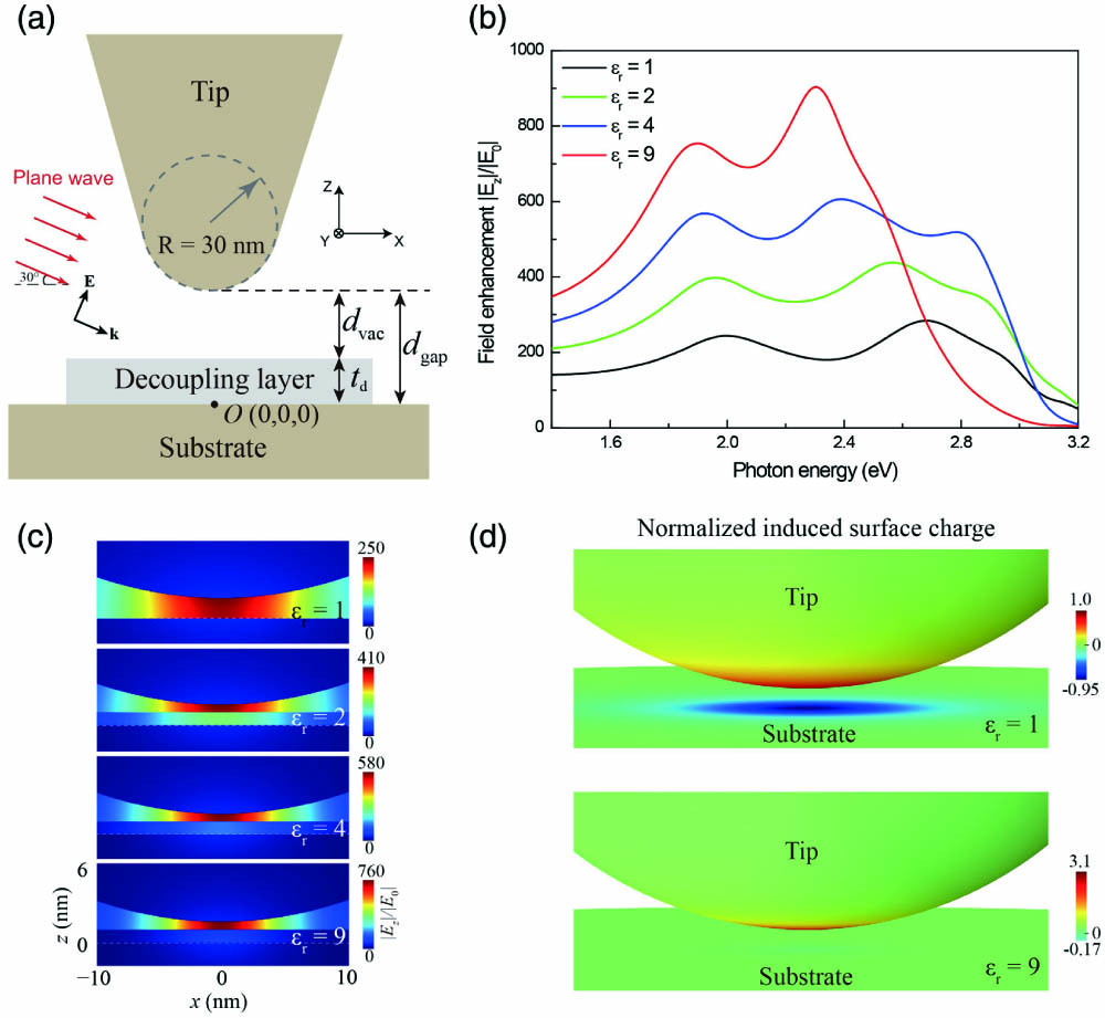
    Fig. 1. (a) Schematic illustration of the model STM junction used for electromagnetic simulations. The tip is modeled as a truncated cone with a radius of 30 nm, a height of 300 nm, and a semi-cone angle of 15°. (b) Local electric field enhancement Mz = |Ez|/|E0| at position (0, 0, 1.2 nm) as a function of incident photon energy for different decoupling layer dielectric constants εr. (c) Spatial distribution of the local electric field enhancement Mz = |Ez|/|E0| in the xz plane (with y = 0) for different dielectric constants εr. (d) Instantaneous induced surface charge density at the surfaces of the tip and the substrate for εr = 1 (upper panel) and εr = 9 (lower panel). The density values are normalized to the maximum value of εr = 1. In (b)–(d), the thickness of the decoupling layer is set to td = 1 nm, and the distance between the tip apex and the top surface of the decoupling layer is set to dvac = 0.6 nm.
    (a) Electric field enhancement Mz = |Ez|/|E0| along the z axis (with x = 0 and y = 0) for different decoupling layer dielectric constants εr. (b) Non-normalized and (c) normalized electric field enhancement Mz = |Ez|/|E0| along the x axis (with y = 0 and z = 1.2 nm). The gap distance is dgap = 1.6 nm, and the decoupling layer thickness is td = 1 nm.
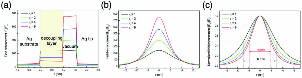
    Fig. 2. (a) Electric field enhancement Mz = |Ez|/|E0| along the z axis (with x = 0 and y = 0) for different decoupling layer dielectric constants εr. (b) Non-normalized and (c) normalized electric field enhancement Mz = |Ez|/|E0| along the x axis (with y = 0 and z = 1.2 nm). The gap distance is dgap = 1.6 nm, and the decoupling layer thickness is td = 1 nm.
    Electric field enhancement with and without a dielectric layer with different thicknesses td and dielectric constants εr. Electric field enhancement |Ez|/|E0| distribution in the xz plane (y = 0) for (a) εr = 1 and (c) εr = 9 with different decoupling layer thicknesses. (b) Enhancement and (d) FWHM of the electric field enhancement |Ez|/|E0| along the x axis (y = 0 and z = td + 0.2 nm) as functions of decoupling layer thickness for four different dielectric constants.
    Fig. 3. Electric field enhancement with and without a dielectric layer with different thicknesses td and dielectric constants εr. Electric field enhancement |Ez|/|E0| distribution in the xz plane (y = 0) for (a) εr = 1 and (c) εr = 9 with different decoupling layer thicknesses. (b) Enhancement and (d) FWHM of the electric field enhancement |Ez|/|E0| along the x axis (y = 0 and z = td + 0.2 nm) as functions of decoupling layer thickness for four different dielectric constants.
    Schematics showing the configurations of (a) a vertical dipole and (d) a horizontal dipole in the model STM junctions. In (a), the shape of the tip and substrate are the same as in Fig. 1(a). In (d), a spherical protrusion with a radius of 0.5 nm is superimposed at the apex of the tip shaft. The quantum efficiency for a vertical dipole on (b) Ag substrate and (c) W substrate and a horizontal dipole on (e) Ag substrate and (f) W substrate with different decoupling layer thicknesses and dielectric constants. In (a)–(f), the vertical dipole–tip distance is 0.4 nm, and the vertical dipole–decoupling-layer distance is 0.2 nm. For a vertical dipole in (a)–(c), the dipole is placed right under the tip apex, while for a horizontal dipole in (d)–(f), the dipole is placed 0.5 nm away laterally from the tip apex.
    Fig. 4. Schematics showing the configurations of (a) a vertical dipole and (d) a horizontal dipole in the model STM junctions. In (a), the shape of the tip and substrate are the same as in Fig. 1(a). In (d), a spherical protrusion with a radius of 0.5 nm is superimposed at the apex of the tip shaft. The quantum efficiency for a vertical dipole on (b) Ag substrate and (c) W substrate and a horizontal dipole on (e) Ag substrate and (f) W substrate with different decoupling layer thicknesses and dielectric constants. In (a)–(f), the vertical dipole–tip distance is 0.4 nm, and the vertical dipole–decoupling-layer distance is 0.2 nm. For a vertical dipole in (a)–(c), the dipole is placed right under the tip apex, while for a horizontal dipole in (d)–(f), the dipole is placed 0.5 nm away laterally from the tip apex.
    Influence of the dielectric constant of the decoupling layer on the TEPL and TERS intensities of a single dipole emitter. (a) TEPL intensity and (b) TERS intensity as functions of the decoupling layer thickness for different dielectric constants. (c) and (d) show the TEPL and TERS images for εr = 1 and εr = 9. In (c) and (d), the molecule is approximated as a vertical dipole, the gap distance is 1.6 nm, the thickness of the decoupling layer is 1 nm, and the plane for simulation of the photon image is z = 1.2 nm.
    Fig. 5. Influence of the dielectric constant of the decoupling layer on the TEPL and TERS intensities of a single dipole emitter. (a) TEPL intensity and (b) TERS intensity as functions of the decoupling layer thickness for different dielectric constants. (c) and (d) show the TEPL and TERS images for εr = 1 and εr = 9. In (c) and (d), the molecule is approximated as a vertical dipole, the gap distance is 1.6 nm, the thickness of the decoupling layer is 1 nm, and the plane for simulation of the photon image is z = 1.2 nm.
    Gong Chen, Jiazhe Zhu, Xiaoguang Li. Influence of a dielectric decoupling layer on the local electric field and molecular spectroscopy in plasmonic nanocavities: a numerical study[J]. Chinese Optics Letters, 2021, 19(12): 123001
    Download Citation