• Chinese Optics Letters
  • Vol. 19, Issue 12, 123001 (2021)
Gong Chen1、2、*, Jiazhe Zhu1, and Xiaoguang Li3、**
Author Affiliations
  • 1School of Physics, Zhengzhou University, Zhengzhou 450052, China
  • 2Hefei National Laboratory for Physical Sciences at the Microscale, University of Science and Technology of China, Hefei 230026, China
  • 3Institute for Advanced Study, Shenzhen University, Shenzhen 518060, China
  • show less
    DOI: 10.3788/COL202119.123001 Cite this Article Set citation alerts
    Gong Chen, Jiazhe Zhu, Xiaoguang Li. Influence of a dielectric decoupling layer on the local electric field and molecular spectroscopy in plasmonic nanocavities: a numerical study[J]. Chinese Optics Letters, 2021, 19(12): 123001 Copy Citation Text show less

    Abstract

    In this Letter, we use electromagnetic simulations to systematically investigate the influence of a thin dielectric layer on the local electric field and molecular spectroscopy in the plasmonic junction. It is found that both the intensity and spatial confinement of the electric field and molecular spectroscopy can be significantly enhanced by applying a dielectric layer with large dielectric constant. We also discuss the optimal dielectric layer thickness to obtain the largest quantum efficiency of a dipole emitter. These results may be instructive for further studies in molecular spectroscopy and optoelectronics in plasmonic junctions.

    1. Introduction

    Single molecules are elementary building blocks for constructing integrated functional devices in the field of organic electronics and optoelectronics. Single-molecule spectroscopy conducted by a scanning tunneling microscope (STM), including STM-induced electroluminescence (STML)[18], tip-enhanced photoluminescence (TEPL)[9], and tip-enhanced Raman spectroscopy (TERS)[1012], is an attractive research area that has caught wide interest in the past decades, and much intriguing information of the molecular scale has been reported. It is known that when molecules are directly adsorbed on the metal surface, the electrons in molecules and the metal surface may strongly hybridize. Consequently, the electronic excitation energy in the molecule can be quickly transferred to the metal and finally lost non-radiatively as heat. To prevent molecular fluorescence quenching and to reduce the perturbation to the molecular orbitals, emitters must be electronically decoupled from the metal surface. In the past decades, diverse experimental strategies have been implemented to prevent fluorescence quenching of quantum emitters in the junction of an STM[13]. A most common strategy is to insert an ultrathin insulating decoupling layer between the emitter and the metal surface to suppress their electronic hybridizations[1,3,13]. Meanwhile, an insulating decoupling layer has also been implemented for TERS measurements of molecules[14]. Although no fluorescence quenching needs to be overcome for TERS, a decoupling layer will reduce the strong hybridization and charge migration between the molecule and the metal substrate, enabling the intrinsic properties of an individual molecule to be ultimately preserved.

    The fluorescence-quenching-suppression effect of an insulating decoupling layer might be attributed to at least two factors. Firstly, the insertion of an insulating decoupling layer will largely block the direct electron hybridization between the molecule and the substrate and thus suppress the ultrafast charge-transfer-induced quenching upon contact. Secondly, the decoupling layer will increase the distance between the molecular emitter and the metal substrate and thus suppress the Ohmic loss induced by the substrate. For practical reasons, one important question is whether and how the thickness and dielectric constant of the decoupling layer affect the molecular fluorescence. Previous STML experiments with single molecules adsorbed on ultrathin insulating NaCl films on Ag(100) surface show that as the thickness of NaCl films grows from two layers to five layers, the electroluminescence intensity grows monotonically, due to the better electronic and electromagnetic decoupling provided by the thicker decoupling layers[5]. But, it remains unclear whether there exists an optimal thickness of the decoupling layer and whether the dielectric constant of the decoupling layer affects the molecular spectroscopy.

    In this Letter, we use classical electromagnetic simulations to systematically study the influence of a thin insulating decoupling layer on the local electric field enhancement and emission properties of a point dipole in the STM tunnel junction. For simplification, we only consider the electromagnetic response of the junction while the electronic structures of the metal junction and the decoupling layer are not considered. Our simulations show that the growth of a decoupling layer on the metal substrate surface will increase both the electric field intensity and lateral spatial confinement, compared to the situation with the same tip–substrate distance but without a decoupling layer. In addition, we find that there exists an optimal decoupling layer thickness to obtain the largest quantum efficiency of a dipole emitter, but this optimal thickness depends on the dielectric constant of the dielectric layer, the materials of the junction, as well as the dipole orientation. Furthermore, the simulations suggest that to obtain stronger molecular photoluminescence intensity and Raman intensity as well as higher spatial resolution, a decoupling layer with a larger dielectric constant is preferred.

    2. Numerical Methods

    We performed electromagnetic simulations using frequency-domain finite-element method based on COMSOL Multiphysics to numerically study the local electric field enhancement and the radiative and non-radiative decay enhancement of an electric dipole emitter in model STM junctions[9,15,16]. As schematically shown in Fig. 1(a), the STM tip is modeled as a truncated cone with a height of 300 nm, within which a sphere with a radius of 30 nm is embedded at its terminal. The substrate is modeled as a hemisphere with a radius of 300 nm. A thin cylinder with a radius of 30 nm, a height of td, and a dielectric constant of εr is constructed above the metal substrate to model the decoupling layer. The region used for electromagnetic simulations is a large sphere with a radius of 900 nm, with perfectly matched layer boundary conditions extending to 1500 nm. The Brendel–Bormann model[17] was used to describe the dielectric responses of the tip and substrate. In this work, the photon energy is set to be 2 eV for εr=1, 1.95 eV for εr=2, and εr=4, 1.9 eV for εr=9, close to the dipolar resonance energy of the junction.

    (a) Schematic illustration of the model STM junction used for electromagnetic simulations. The tip is modeled as a truncated cone with a radius of 30 nm, a height of 300 nm, and a semi-cone angle of 15°. (b) Local electric field enhancement Mz = |Ez|/|E0| at position (0, 0, 1.2 nm) as a function of incident photon energy for different decoupling layer dielectric constants εr. (c) Spatial distribution of the local electric field enhancement Mz = |Ez|/|E0| in the xz plane (with y = 0) for different dielectric constants εr. (d) Instantaneous induced surface charge density at the surfaces of the tip and the substrate for εr = 1 (upper panel) and εr = 9 (lower panel). The density values are normalized to the maximum value of εr = 1. In (b)–(d), the thickness of the decoupling layer is set to td = 1 nm, and the distance between the tip apex and the top surface of the decoupling layer is set to dvac = 0.6 nm.

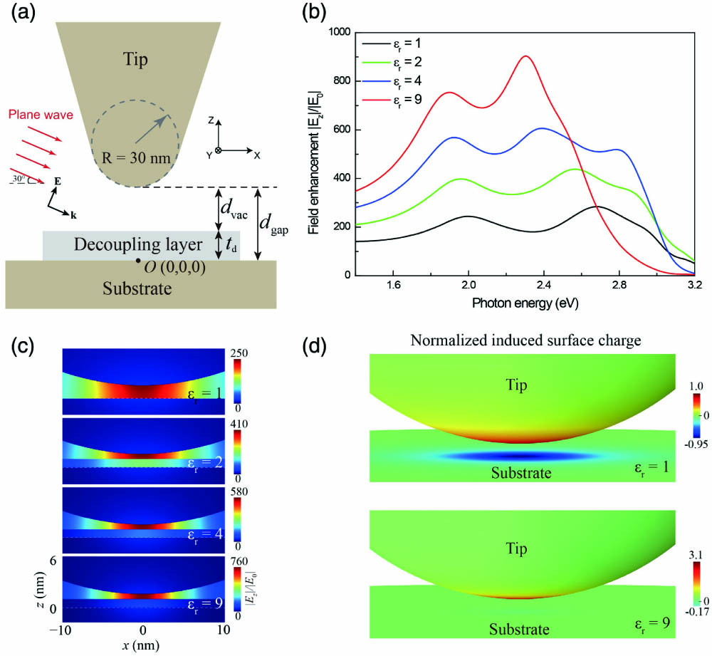
    Figure 1.(a) Schematic illustration of the model STM junction used for electromagnetic simulations. The tip is modeled as a truncated cone with a radius of 30 nm, a height of 300 nm, and a semi-cone angle of 15°. (b) Local electric field enhancement Mz = |Ez|/|E0| at position (0, 0, 1.2 nm) as a function of incident photon energy for different decoupling layer dielectric constants εr. (c) Spatial distribution of the local electric field enhancement Mz = |Ez|/|E0| in the xz plane (with y = 0) for different dielectric constants εr. (d) Instantaneous induced surface charge density at the surfaces of the tip and the substrate for εr = 1 (upper panel) and εr = 9 (lower panel). The density values are normalized to the maximum value of εr = 1. In (b)–(d), the thickness of the decoupling layer is set to td = 1 nm, and the distance between the tip apex and the top surface of the decoupling layer is set to dvac = 0.6 nm.

    The quantum efficiency of a point dipole is calculated as follows. We first calculate the electromagnetic fields in space for a point dipole placed at a position r. Then, the radiation power Prad to the far field from the dipole is calculated through integrating the time-averaged Poynting vector (S=12{E×H*}) over the boundary of the simulation region, where E and H represent the electric and magnetic fields, respectively. The non-radiative power Pnon-rad is calculated through integrating the power dissipation density (12σ|E|2) over the volumes of the tip and substrate, where σ represents their conductivity. Then, the quantum efficiency is evaluated as η=Prad/(Prad+Pnonrad).

    3. Results and Discussions

    Surface plasmons have been widely used to enhance weak optical signals, e.g.,  from molecules[18,19] and hot electrons[20]. It is known that the plasmonic response of metal structures is sensitive to the dielectric environment[21]. In STM junctions, the strength and spatial distribution of the plasmonic fields are not determined by the tip itself but can be strongly influenced by the substrate[22,23]. The electric field can be orders of magnitude larger for a metal substrate than for a dielectric substrate[9,24]. The effect of the substrate can be rationalized by considering that the oscillating charge in the tip induces a mirror charge distribution in the substrate that can further increase the local field intensity in the gap region. In addition, the electromagnetic coupling between the oscillating charges in the tip and in the substrate could change the plasmon resonance of the junction. The capability of the substrate to support this image charge is determined by its dielectric function and is thus sensitive to the dielectric adsorptions.

    We first study the influence of the dielectric constant εr of the decoupling layer on the electric field enhancement in the model STM junction under plane wave illumination. As schematically illustrated in Fig. 1(a), a p-polarized plane wave with an incident angle of 60° with respect to the surface normal is used as an excitation source. We define the local electric field enhancement factor Mz(r)=|Ez(r)|/|E0|, where Ez(r) is the vertical component of the local electric field at position r, and E0 is the electric field of the incident plane wave. When the dielectric constant of the decoupling layer is set to εr=1, the plasmonic nanocavity exhibits two clear resonance peaks at 2eV and 2.7eV, which can be attributed to the dipolar and quadrupolar modes, respectively [Fig. 1(b)][25]. As the thickness of the decoupling layer is kept as a constant value of td=1nm but the dielectric constant εr is increased from 1 to 9, both the dipolar and quadrupolar nanocavity plasmon modes gradually redshift, and the local field enhancement Mz(r) increases significantly, as the decoupling layer affects the hybridization of the tip and substrate. The spatial distribution of the field enhancement in the xz plane (with y=0) for different εr is shown in Fig. 1(c). It can be seen that as εr is increased but the distance between the surfaces of the tip and substrate (i.e., gap distance dgap) is kept constant, the local electric field in the vacuum region becomes more intense and more spatially confined both vertically and laterally. Meanwhile, the electric field inside the dielectric layer becomes increasingly weaker. The induced surface charge densities at the surfaces of the tip and the substrate for εr=1 and εr=9, which will help to understand the plasmonic hybridization, are shown in the upper and lower panels of Fig. 1(d).

    The phenomenon that the electric field is enhanced in the vacuum but weakened inside the decoupling layer is more clearly illustrated in Fig. 2(a), where the local electric field enhancement Mz along the z axis (with x=0 and y=0) is shown. Here, the positions at z=0nm, z=1.0nm, and z=1.6nm correspond to the substrate surface, the upper surface of the decoupling layer, and the tip apex, respectively. When εr=1, the electric field in the gap region is vertically continuous. In addition, the electric field is with almost the same intensity close to the tip surface (z=0) and the substrate surface (z=1.6nm) since the tip radius is much larger than the gap distance. This is further supported by the spatial distribution of the normalized induced surface charge densities σind(r) for εr=1 in the lower panel of Fig. 1(d), from which we can see that the maximum value of |σind(r)| is almost identical at the tip apex and at the substrate surface (all charge density values are normalized to the maximum value of εr=1). However, as εr becomes larger than one, the electric field becomes discontinuous at the interface between the vacuum and the dielectric layer (i.e., at the z=1nm plane): the electric field is stronger in the vacuum region but weaker in the decoupling layer. As εr is further increased, the discontinuity becomes increasingly more significant. Indeed, the continuous condition requires that the normal component of the electric displacement be continuous at the interface and thus Ez,vac=εrEz,d, where Ez,vac and Ez,d are the z components of the electric field in the vacuum and in the decoupling layer, respectively. Therefore, the electric field in the vacuum region will approximately be εr times as large as the electric field in the decoupling layer, as can be verified in Fig. 2(b). As shown in the lower panel of Fig. 1(d), the maximum value of |σind(r)| at the tip terminal is increased by over 210%, while it is decreased by over 80% at the substrate surface when εr is increased from 1 to 9. In other words, one can say that as the dielectric constant of the decoupling layer increases, the electric field at the dielectric/substrate interface is more strongly screened, and thus the induced surface charge at this interface decreases. Meanwhile, σind(r) becomes more localized in the junction. In addition, with the increment of εr, not only the intensity of the electric field becomes stronger but its lateral spatial distribution also becomes more confined both horizontally and vertically in the vacuum region. As shown in Fig. 2(d), as εr increases from 1 to 9, the full width at half-maximum (FWHM) of Mz in the lateral direction decreases from 14.6 nm to 9.2 nm. This is because as εr is increased, the electric field is more confined in the vacuum region between the tip and the decoupling layer, which is evidently smaller than the region between the tip and substrate. This decreases the vertical and horizontal spatial extension of the electric field and increases the electric field energy density, generating electric fields with higher intensity and smaller FWHM.

    (a) Electric field enhancement Mz = |Ez|/|E0| along the z axis (with x = 0 and y = 0) for different decoupling layer dielectric constants εr. (b) Non-normalized and (c) normalized electric field enhancement Mz = |Ez|/|E0| along the x axis (with y = 0 and z = 1.2 nm). The gap distance is dgap = 1.6 nm, and the decoupling layer thickness is td = 1 nm.

    Figure 2.(a) Electric field enhancement Mz = |Ez|/|E0| along the z axis (with x = 0 and y = 0) for different decoupling layer dielectric constants εr. (b) Non-normalized and (c) normalized electric field enhancement Mz = |Ez|/|E0| along the x axis (with y = 0 and z = 1.2 nm). The gap distance is dgap = 1.6 nm, and the decoupling layer thickness is td = 1 nm.

    In tip-enhanced single-molecule spectroscopy experiments, a larger electric enhancement and a better spatial confinement of the local electric field are usually in demand, since the former is usually related to the intensity, while the latter is related to the spatial resolution of molecular spectroscopy measurements. To achieve these goals, one could usually employ a sharper tip or decrease the gap distance. However, the introduction of the decoupling layer usually prevents one from shrinking the gap distance to extremely small values. Our calculations suggest that increasing the dielectric constant of the decoupling layer will help to increase the field enhancement and spatial confinement, although the distance between the surfaces of the metal tip and the metal substrate is still kept at a relatively large value.

    In addition to the dielectric constant εr, the thickness of the dielectric layer td could also affect the intensity and the lateral spatial confinement of the local electric fields. In Fig. 3, the distance between the tip apex and the upper surface of the decoupling layer is set to be dvac=0.6nm, so the gap distance dgap is 0.6 nm larger than the thickness td of the decoupling layer: dgap=td+0.6nm. As shown in Fig. 3(a), when εr=1, as the thickness of the decoupling layer increases (this is equivalent to increasing the gap distance), the field enhancement |Ez|/|E0| quickly decreases, and the field becomes laterally less confined. Specifically, increasing the gap distance from 0.6 nm to 3.6 nm will dramatically decrease the field enhancement from 853 to 97 [Figs. 3(a) and 3(b)], while significantly increasing the FWHM of Mz from 8.0nm to 23.2nm. This is because the increment of the gap distance increases the effective volume of the plasmonic nanocavity, which will not only make the electromagnetic fields less confined both vertically and horizontally, but also reduce the local electromagnetic density and thus decrease the electric field intensity. On the other hand, if we choose a dielectric layer with a large dielectric constant of εr=9, as td is increased from 0 to 3 nm, the field enhancement is reduced from 853 to 548, while the FWHM of Mz is only increased from 8.0nm to 10.7nm [Figs. 3(c) and 3(d)]. As illustrated, the reductions of the field intensity and lateral spatial confinement are much less significant with the increment of the gap distance if εr is large.

    Electric field enhancement with and without a dielectric layer with different thicknesses td and dielectric constants εr. Electric field enhancement |Ez|/|E0| distribution in the xz plane (y = 0) for (a) εr = 1 and (c) εr = 9 with different decoupling layer thicknesses. (b) Enhancement and (d) FWHM of the electric field enhancement |Ez|/|E0| along the x axis (y = 0 and z = td + 0.2 nm) as functions of decoupling layer thickness for four different dielectric constants.

    Figure 3.Electric field enhancement with and without a dielectric layer with different thicknesses td and dielectric constants εr. Electric field enhancement |Ez|/|E0| distribution in the xz plane (y = 0) for (a) εr = 1 and (c) εr = 9 with different decoupling layer thicknesses. (b) Enhancement and (d) FWHM of the electric field enhancement |Ez|/|E0| along the x axis (y = 0 and z = td + 0.2 nm) as functions of decoupling layer thickness for four different dielectric constants.

    Previous STML experiments for single molecules on ultrathin NaCl films suggested that as the thickness of the NaCl decoupling layer grows from two layers to five layers, the fluorescence intensity grows monotonically[5]. However, it remains unclear whether there exists an optimal thickness of the decoupling layer or whether and how the dielectric constant of the decoupling layer affects the emission properties. Here, we numerically study the quantum efficiency of an electric dipole emitter with either vertical [Figs. 4(a)4(c)] or horizontal [Figs. 4(d)4(f)] orientations placed on a decoupling layer with different thicknesses td and dielectric constants εr. As shown in Fig. 4(b), the quantum efficiency of a vertical dipole with the Ag substrate is comparatively large, even when the distance between the dipole and the substrate is very small (i.e., very small td). This is because for the Ag plasmonic nanocavity with a very small gap distance, the vertical component of the electric field Ez is extremely strong [see, e.g.,  Figs. 1(b) and 1(c)]. The effective coupling between Ez and the vertical dipole enables the radiative decay rate of the dipole to be comparable to the non-radiative decay rate, and thus the dipole emission is not quenched[9,26]. A thicker decoupling layer may even decrease rather than increase η due to the decreasing of the electric field with the increasing gap distance.

    Schematics showing the configurations of (a) a vertical dipole and (d) a horizontal dipole in the model STM junctions. In (a), the shape of the tip and substrate are the same as in Fig. 1(a). In (d), a spherical protrusion with a radius of 0.5 nm is superimposed at the apex of the tip shaft. The quantum efficiency for a vertical dipole on (b) Ag substrate and (c) W substrate and a horizontal dipole on (e) Ag substrate and (f) W substrate with different decoupling layer thicknesses and dielectric constants. In (a)–(f), the vertical dipole–tip distance is 0.4 nm, and the vertical dipole–decoupling-layer distance is 0.2 nm. For a vertical dipole in (a)–(c), the dipole is placed right under the tip apex, while for a horizontal dipole in (d)–(f), the dipole is placed 0.5 nm away laterally from the tip apex.

    Figure 4.Schematics showing the configurations of (a) a vertical dipole and (d) a horizontal dipole in the model STM junctions. In (a), the shape of the tip and substrate are the same as in Fig. 1(a). In (d), a spherical protrusion with a radius of 0.5 nm is superimposed at the apex of the tip shaft. The quantum efficiency for a vertical dipole on (b) Ag substrate and (c) W substrate and a horizontal dipole on (e) Ag substrate and (f) W substrate with different decoupling layer thicknesses and dielectric constants. In (a)–(f), the vertical dipole–tip distance is 0.4 nm, and the vertical dipole–decoupling-layer distance is 0.2 nm. For a vertical dipole in (a)–(c), the dipole is placed right under the tip apex, while for a horizontal dipole in (d)–(f), the dipole is placed 0.5 nm away laterally from the tip apex.

    However, when the vertical dipole is placed above a more lossy W substrate, choosing a proper decoupling layer thickness becomes more important [Fig. 4(c)]. When the thickness td is very small, the non-radiative channels induced by the lossy W substrate will largely decrease η. As td is increased, the distance between the dipole and the substrate is increased, and the quantum efficiency first increases and then decreases, showing an optimal value that is sensitive to εr. For example, the optimal thickness to reach the largest η is td0.9nm for εr=1, further increasing t will decrease rather than increase η. The optimal thickness grows with increasing εr. For εr=9, further increasing td will not decrease η. This is because, when εr is large enough, the electric field is primarily confined within the small region between the tip terminal and the upper surface of the decoupling layer, and thus the electromagnetic energy density is not much decreased with increasing decoupling layer thickness, as we have already learned from Fig. 3. In other words, the plasmonic nanocavity formed by a metal tip and a dielectric substrate with large dielectric constant can induce large field intensity and sustain relatively efficient molecular emission.

    Considering that many STML experiments were carried out for molecules with transition dipoles oriented parallel to the substrate, we also calculate the dependence of the quantum efficiency on the dielectric constant and thickness of the decoupling layer for a horizontal dipole [see Fig. 4(d) for schematic illustration]. To ensure comparatively large quantum efficiency, a spherical protrusion with a radius of 0.5 nm is superimposed at the apex of the tip shaft, and the horizontal dipole is laterally placed 0.5 nm away from the tip apex, following Ref. [9]. It is worthwhile to note that the protrusion at the tip apex is essentially important in preventing the emission from dipoles that are oriented parallel to the substrate from quenching. Moreover, to ensure an effective coupling between the horizontal dipole and the nanocavity plasmon, the dipole is placed 0.5 nm away laterally from the tip apex[9]. We found that the overall tendency for the horizontal dipole is similar to that of the vertical dipole except the quantum efficiency is lower. In addition, the optimal value of the decoupling layer thickness is slightly different. As a short summary, the optimal thickness to obtain the maximum quantum efficiency depends on the dielectric constant of the decoupling layer, the material of the substrate, as well as the dipole orientation. For the substrate with small dielectric loss, a dielectric layer with a thickness of ∼1 nm or below will give the largest quantum efficiency, while for the substrate with large dielectric loss, a thicker decoupling layer might be better. However, it should be noted that some other factors, such as electronic hybridization, electron tunneling, and quantum corrections to the dielectric responses[27], could further suppress the molecular emission, but these effects are not taken into account in the classical electromagnetic calculations.

    Finally, we briefly discuss the influence of the thickness td and dielectric constant εr of the decoupling layer on the intensity of single-molecule TEPL and TERS. In the calculations of Fig. 5, the TEPL intensity is approximated as ITEPL|Ez|2/|E0|2×η, and the TERS intensity is approximated as ITERS|Ez|4/|E0|4. As shown in Figs. 5(a) and 5(b), both the intensities of TEPL and TERS show a strong dependence on the thickness td and dielectric constant εr of the decoupling layer. For εr=1, as the decoupling layer thickness is increased from 0.2 nm to 5 nm, the TEPL and TERS intensities, respectively, decrease by 3 and 4 orders of magnitude due to the much weaker electric field in larger gaps. However, as εr is increased, the decrease of TEPL and TERS intensities with increasing decoupling layer thickness becomes much slower. Moreover, at a fixed decoupling layer thickness, both the TEPL and TERS intensities become larger for larger εr, especially when td is large. As shown in the simulated single-molecule TEPL and TERS photon images in Figs. 5(c) and 5(d), for a fixed value of td=1nm, as εr is increased from 1 to 9, the TEPL intensity increases by 17 times, and the TERS intensity increases by 92 times. Moreover, the photon images become more spatially confined, suggesting that applying a decoupling layer with larger dielectric constant could further improve the spatial resolution of single-molecule TEPL and TERS imaging. Thus, it is believed that a dielectric layer with larger εr is very helpful to increase the intensities as well as the spatial confinement of STML, TEPL, and TERS of individual molecules.

    Influence of the dielectric constant of the decoupling layer on the TEPL and TERS intensities of a single dipole emitter. (a) TEPL intensity and (b) TERS intensity as functions of the decoupling layer thickness for different dielectric constants. (c) and (d) show the TEPL and TERS images for εr = 1 and εr = 9. In (c) and (d), the molecule is approximated as a vertical dipole, the gap distance is 1.6 nm, the thickness of the decoupling layer is 1 nm, and the plane for simulation of the photon image is z = 1.2 nm.

    Figure 5.Influence of the dielectric constant of the decoupling layer on the TEPL and TERS intensities of a single dipole emitter. (a) TEPL intensity and (b) TERS intensity as functions of the decoupling layer thickness for different dielectric constants. (c) and (d) show the TEPL and TERS images for εr = 1 and εr = 9. In (c) and (d), the molecule is approximated as a vertical dipole, the gap distance is 1.6 nm, the thickness of the decoupling layer is 1 nm, and the plane for simulation of the photon image is z = 1.2 nm.

    4. Conclusion

    In this work, we have used electromagnetic simulations to numerically study the influence of a thin dielectric decoupling layer on the local field enhancement and molecular spectroscopy intensity in the junction of an STM. Our simulations show that the growth of a decoupling layer on the metal substrate surface will increase both the electric field intensity and lateral spatial confinement, compared to the situation with the same tip–substrate distance but without a decoupling layer. In addition, we find that there exists an optimal decoupling layer thickness to obtain the largest quantum efficiency of a dipole emitter, but this optimal thickness depends on the dielectric constant of the dielectric layer, the materials of the junction, as well as the dipole orientation. To obtain higher molecular photoluminescence, Raman intensities, and spatial resolution, a decoupling layer with a larger dielectric constant is preferred. These results may be instructive for further studies in molecular optics and optoelectronics in plasmonic junctions.

    References

    [1] X. H. Qiu, G. V. Nazin, W. Ho. Vibrationally resolved fluorescence excited with submolecular precision. Science, 299, 542(2003).

    [2] Z. C. Dong, X. L. Guo, A. S. Trifonov, P. S. Dorozhkin, K. Miki, K. Kimura, S. Yokoyama, S. Mashiko. Vibrationally resolved fluorescence from organic molecules near metal surfaces in a scanning tunneling microscope. Phys. Rev. Lett., 92, 086801(2004).

    [3] Y. Zhang, Y. Luo, Y. Zhang, Y. J. Yu, Y. M. Kuang, L. Zhang, Q. S. Meng, Y. Luo, J. L. Yang, Z. C. Dong, J. G. Hou. Visualizing coherent intermolecular dipole-dipole coupling in real space. Nature, 531, 623(2016).

    [4] H. Imada, K. Miwa, M. Imai-Imada, S. Kawahara, K. Kimura, Y. Kim. Real-space investigation of energy transfer in heterogeneous molecular dimers. Nature, 538, 364(2016).

    [5] L. Zhang, Y. J. Yu, L. G. Chen, Y. Luo, B. Yang, F. F. Kong, G. Chen, Y. Zhang, Q. Zhang, Y. Luo, J. L. Yang, Z. C. Dong, J. G. Hou. Electrically driven single-photon emission from an isolated single molecule. Nat. Commun., 8, 580(2017).

    [6] B. Doppagne, M. C. Chong, H. Bulou, A. Boeglin, F. Scheurer, G. Schull. Electrofluorochromism at the single-molecule level. Science, 361, 251(2018).

    [7] G. Chen, Y. Luo, H. Gao, J. Jiang, Y. Yu, L. Zhang, Y. Zhang, X. Li, Z. Zhang, Z. Dong. Spin-triplet-mediated up-conversion and crossover behavior in single-molecule electroluminescence. Phys. Rev. Lett., 122, 177401(2019).

    [8] Y. Luo, G. Chen, Y. Zhang, L. Zhang, Y. Yu, F. Kong, X. Tian, Y. Zhang, C. Shan, Y. Luo, J. Yang, V. Sandoghdar, Z. Dong, J. G. Hou. Electrically driven single-photon superradiance from molecular chains in a plasmonic nanocavity. Phys. Rev. Lett., 122, 233901(2019).

    [9] B. Yang, G. Chen, A. Ghafoor, Y. Zhang, Y. Zhang, Y. Zhang, Y. Luo, J. Yang, V. Sandoghdar, J. Aizpurua, Z. Dong, J. G. Hou. Sub-nanometre resolution in single-molecule photoluminescence imaging. Nat. Photon., 14, 693(2020).

    [10] R. Zhang, Y. Zhang, Z. C. Dong, S. Jiang, C. Zhang, L. G. Chen, L. Zhang, Y. Liao, J. Aizpurua, Y. Luo, J. L. Yang, J. G. Hou. Chemical mapping of a single molecule by plasmon-enhanced Raman scattering. Nature, 498, 82(2013).

    [11] Y. Zhang, B. Yang, A. Ghafoor, Y. Zhang, Y.-F. Zhang, R.-P. Wang, J.-L. Yang, Y. Luo, Z.-C. Dong, J. G. Hou. Visually constructing the chemical structure of a single molecule by scanning Raman picoscopy. Natl. Sci. Rev., 6, 1169(2019).

    [12] J. Lee, K. T. Crampton, N. Tallarida, V. A. Apkarian. Visualizing vibrational normal modes of a single molecule with atomically confined light. Nature, 568, 78(2019).

    [13] K. Kuhnke, C. Grosse, P. Merino, K. Kern. Atomic-scale imaging and spectroscopy of electroluminescence at molecular interfaces. Chem. Rev., 117, 5174(2017).

    [14] R. B. Jaculbia, H. Imada, K. Miwa, T. Iwasa, M. Takenaka, B. Yang, E. Kazuma, N. Hayazawa, T. Taketsugu, Y. Kim. Single-molecule resonance Raman effect in a plasmonic nanocavity. Nat. Nanotechnol., 15, 105(2020).

    [15] A. Downes, D. Salter, A. Elfick. Finite element simulations of tip-enhanced Raman and fluorescence spectroscopy. J. Phys. Chem. B, 110, 6692(2006).

    [16] Y. Wei, H. Pei, D. Sun, S. Duan, G. Tian. Numerical investigations on the electromagnetic enhancement effect to tip-enhanced Raman scattering and fluorescence processes. J. Phys. Condens. Matter., 31, 235301(2019).

    [17] A. D. Rakić, A. B. Djurišić, J. M. Elazar, M. L. Majewski. Optical properties of metallic films for vertical-cavity optoelectronic devices. Appl. Opt., 37, 5271(1998).

    [18] C. Wu, N. Liu, H. Hu, X. Guo, B. Liao, J. Liu, L. Wang, C. Chen, X. Yang, Q. Dai. Detecting molecular vibrational modes of side chains and endpoints in nanoscale proteins with graphene plasmon. Chin. Opt. Lett., 17, 062401(2019).

    [19] Y. Dong, Q. Yang, G. Du, F. Chen, N. Uddin, D. Lankanath, X. Hou. Electronic manipulation of near-field nanofocusing in few-layer graphene-based hybrid nanotips. Chin. Opt. Lett., 17, 072501(2019).

    [20] Z. Yang, K. Du, W. Zhang, S. Chua, T. Mei. A polarization-insensitive fishnet/spacer/mirror plasmonic absorber for hot electron photodetection application. Chin. Opt. Lett., 18, 052402(2020).

    [21] J. M. Pitarke, V. M. Silkin, E. V. Chulkov, P. M. Echenique. Theory of surface plasmons and surface-plasmon polaritons. Rep. Prog. Phys., 70, 1(2007).

    [22] I. Notingher, A. Elfick. Effect of sample and substrate electric properties on the electric field enhancement at the apex of SPM nanotips. J. Phys. Chem. B, 109, 15699(2005).

    [23] N. Mauser, A. Hartschuh. Tip-enhanced near-field optical microscopy. Chem. Soc. Rev., 43, 1248(2014).

    [24] J. R. Isaac, H. Xu. Fluorescence enhancement and quenching in tip-enhanced fluorescence spectroscopy. OSA Continuum, 1, 899(2018).

    [25] A. Martin-Jimenez, A. I. Fernandez-Dominguez, K. Lauwaet, D. Granados, R. Miranda, F. J. Garcia-Vidal, R. Otero. Unveiling the radiative local density of optical states of a plasmonic nanocavity by STM. Nat. Commun., 11, 1021(2020).

    [26] R. Faggiani, J. Yang, P. Lalanne. Quenching, plasmonic, and radiative decays in nanogap emitting devices. ACS Photonics, 2, 1739(2015).

    [27] W. Zhu, R. Esteban, A. G. Borisov, J. J. Baumberg, P. Nordlander, H. J. Lezec, J. Aizpurua, K. B. Crozier. Quantum mechanical effects in plasmonic structures with subnanometre gaps. Nat. Commun., 7, 11495(2016).

    Gong Chen, Jiazhe Zhu, Xiaoguang Li. Influence of a dielectric decoupling layer on the local electric field and molecular spectroscopy in plasmonic nanocavities: a numerical study[J]. Chinese Optics Letters, 2021, 19(12): 123001
    Download Citation