
Yong Chen, Yang Zhao, Qiufeng Ye, Zema Chu, Zhigang Yin, Xingwang Zhang, Jingbi You. Improved efficiency and photo-stability of methylamine-free perovskite solar cells via cadmium doping[J]. Journal of Semiconductors, 2019, 40(12): 122201
- Journal of Semiconductors
- Vol. 40, Issue 12, 122201 (2019)
Abstract
1. Introduction
Organic–inorganic hybrid metal halide perovskite solar cells have become popular in solar cells in recent years due to their low cost and high-power conversion efficiency[
In this manuscript, a methylamine-free perovskite CsxFA1-xPbI3 was synthesized by one-step method and the solar cell delivered a remarkable efficiency beyond 20%. In addition, we incorporated smaller cadmium ions into B site of perovskite to partially replace the Pb ions, the crystallinity has been improved and the charge carrier lifetime has been extended. Consequently, the solar cells with Cd showed 20.59% PCE and, more importantly, the photo-stability of perovskite solar cell has been significantly improved.
2. Experimental
2.1. Materials
The SnO2 colloid precursor was obtained from alfa aesar (tin (IV) oxide), dimethylformamide (DMF), dimethyl sulfoxide (DMSO) and chlorobenzene (CB) were purchased from alfa aesar. Anhydrous lead iodide (PbI2), cadmium iodide (CdI2) and cesium chloride (CsCl), were obtained from Sigma Aldrich. Formamidine iodide (FAI), formamidine chloride (FACl) were purchased from Xi’an Polymer Light Technology Corp.
2.2. Perovskite solar cells fabrication
ITO glass was cleaned by sequentially washing with detergent, deionized (DI) water, acetone, and isopropanol (IPA). Before spinning, the ITO was cleaned by UVO for 10 min. A compact thin layer of SnO2 nanoparticle film was then spin coated at 4000 rpm for 30 s, subsequently annealed on a hot plate at 150 °C for 20 min in ambient air. Perovskite precursors with and without Cd doping were prepared. For the control precursor, the molar ratios of PbI2 : FAI : FACl : CsCl are 1.55 : 1.5 : 0.3 : 0.1. For the precursor with Cd doping, a 2% molar of CdI2 had been introduced. These materials were dissolved in a mixture solvent (DMSO : DMF = 9 : 1). The precursor solutions were then spin coated onto the SnO2 layer at the speed of 2000 rpm for 60 s by one-step process, and chlorobenzene (200 μL) was dropped on the perovskite films surface as anti-solvent at the speed of 5000 rpm for 30 s. The films were then annealed at 150 °C for 20 min in ambient air (30%–40% humidity). The hole transporting layer was then spin coated on top of the perovskite film at the speed of 2000 rpm for 30 s using 2,2′,7,7′-tetrakis(N,N-dip-methoxyphenylamine)-9,9′-spirobifluorene (Spiro-OMeTAD) solution. 1 mL Spiro-OMeTAD solution consisted of 72.3 mg Spiro-OMeTAD, 35 μL bis(trifluoromethane) sulfonimide lithium salt (Li-TFSI) stock solution (260 mg Li-TFSI in 1 mL acetonitrile), 30 μL 4-tertbutylpyridine, and 1 mL chlorobenzene. Finally, 100 nm of Au counter electrode was thermal evaporated on top of hole transporting layer using a shadow mask. The effective area of the device was 0.108 cm2 and a 0.0737 cm2 metal mask was used to define the accurate active cell area.
2.3. Device characterization
The morphology of perovskite films was measured by a field-emission scanning electron microscopy (FEI NanoSEM650), using an electron beam accelerated at 0.5 to 30 kV, enabling operation at various currents. The X-ray diffraction (XRD) patterns (θ–2θ scans) of the perovskite films were collected with a Rigaku D/MAX-2500 system, using Cu Kα (λ = 1.5405 Å) at 40 kV and 200 mA. Steady state photoluminescence (PL) measurement was conducted by FLS980 spectrometer (Edinburgh, England), Time-resolved photoluminescence (TRPL) was measured by Edinburgh F900 spectrometer (England), both PL and TRPL were manipulated in ambient air. X-ray photoelectron spectroscopy (XPS) was carried out using the Thermo Scientific ESCALab 250Xi system, with 200 W monochromated Al Kα (1486.6 eV) radiation and a 500 nm X-ray spot. The J–V characteristics of the photovoltaic cells were measured using the Keithley 2400 source meter, under simulated one-sun AM 1.5 G illumination with a solar simulator (Enli Technology, Taiwan). The light intensity was calibrated by KG-5 Si diode. The external quantum efficiency (EQE) was manipulated using an Enli Tech (Taiwan) measurement system. The illumination stability test was carried out in the nitrogen glove box and white LED arrays were used for continuous illumination.
3. Results and discussions
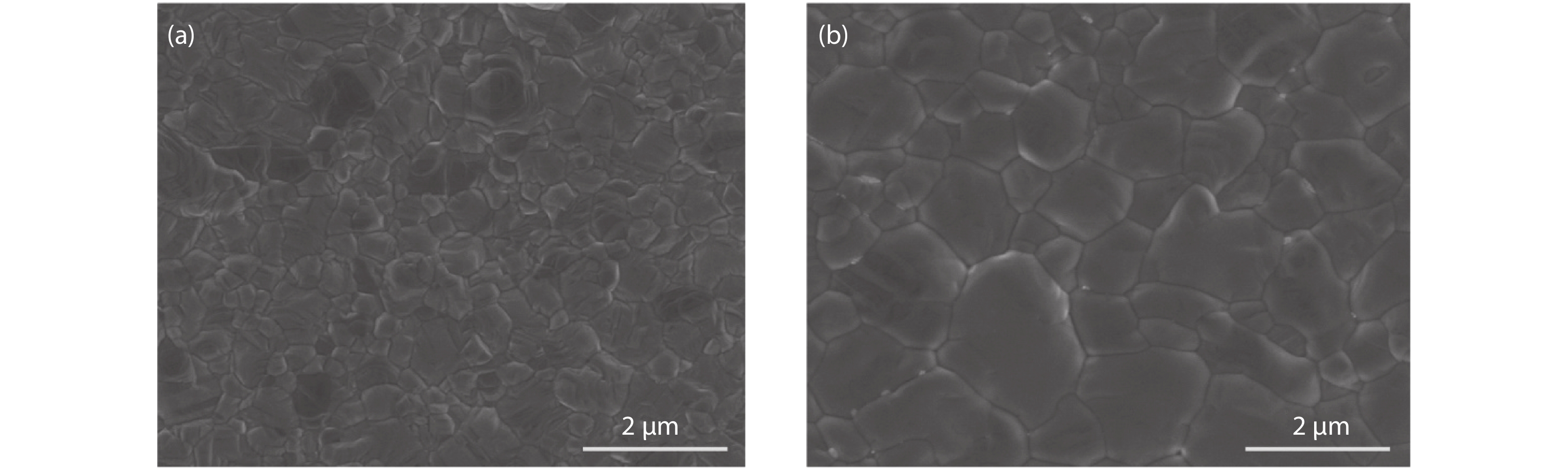
We have checked the morphology of perovskite films with and without CdI2 by scanning electron microscopy (SEM). As shown in Fig. 1(a), the perovskite film without CdI2 is very uniform and the crystal size is about 500 nm. The introduction of Cl ions in the precursor could assist the growth of the perovskite crystallinity[
![]()
Figure 1.The morphology of perovskite films with and without Cd doping.
To study the influence of Cd incorporation on the growth of perovskite crystals, X-ray diffraction measurement has been carried out. From the Fig. 2(a), we can find that the XRD peaks of the film without CdI2 are mostly from the perovskite diffraction patterns and only a small amount of PbI2 are observed. The intensity of XRD diffraction peaks of the perovskite film with CdI2 has been greatly improved, which indicates that the crystallinity of perovskite films has been promoted, which is consistent with the SEM results. In addition, the diffraction peaks of PbI2 has also been enhanced in the films with CdI2, indicating more residual PbI2 in the film. This can be explained because CdI2 has occupied the PbI2 site.
![]()
Figure 2.(Color online) Crystal characteristic and optoelectronic properties of perovskite films with and without Cd doping. (a) X-ray diffraction (XRD) of the perovskite films with and without Cd doing. (b) X-ray photoelectron spectroscopy (XPS) of the perovskite film with Cd doping. The Cd 3d core energy level was recorded. (c) Photoluminescence of the perovskite films with and without Cd doping. (d) Time-resolved photoluminescence (TRPL) of the perovskite films with and without Cd doping.
More importantly, we have observed that the diffraction angles from perovskite diffraction patterns in the film with CdI2 have shifted to smaller angles. For example, the diffraction angles of (100) plane has shifted from 14° to 13.96° (Inset of Fig. 2(a)). According to the Bragg equation 2dsinθ = nλ, and it is concluded that the perovskite lattice constant of thin film with CdI2 is larger than that of thin film without CdI2. This could be due to the lattice strain relaxation: the lattice strain originates from the ionic size mismatch between the A cation and the lead halide cage size, resulting in perovskite structure distortions and BX6 octahedra tilting[
X-ray photoelectron spectroscopy (XPS) was carried out to check the existence of Cd in the perovskite films, the Cd 3d core energy level has been tracked and it is found that there are two strong peaks located at 405.6 and 412.5 eV, which correspond to the Cd 3d5/2 and Cd 3d3/2, respectively. This result confirms that the existence of Cd in the perovskite films.
We checked the steady photoluminescence (PL) of the perovskite films with and without CdI2 (Fig. 2(c)), we found that the PL intensities are obviously increased after introducing CdI2 into perovskite, this could be due to the improvement of crystallinity of perovskite films (Fig. 1).
We also found the PL spectra peak of perovskite film has a slightly red shift and the result can be explained by the perovskite film with CdI2 has a lower band gap value. Due to the perovskite film without CdI2 trend to be the tetragonal phase under the excessive lattice strain as a result of the ionic size mismatch[
To further explore the charge carrier, time-resolved photoluminescence (TRPL) was then carried out. As shown in Fig. 2(d), the perovskite film with CdI2 shows significantly slower PL decay than that of perovskite film without CdI2. The decay lifetime of perovskite film is considered as a key indicator of the deposited films quality: a longer carrier lifetime means better crystalline and lower defect density. To study the carrier lifetime quantitatively, the kinetics of charge carrier recombination be established by the follow kinetic equation. We use a bi-exponential decays[
The fitted results are shown in Table 1. In this kinetic decay model, the fast component τ1 was usually related to carrier recombination caused by surface defects, and the slow component τ2 was related to recombination caused by bulk perovskite defects. Photo-generated carriers was formed in perovskite films under laser excitation. Because there is no transporting layer, the extraction process cannot have happened and the photo-generated carriers have only recombined through radiative recombination and non-radiative recombination. The two processes are opposite, the former goes through the energy loss process through emission, while the latter goes through the energy loss process in the form of recombination with defects etc. Under this open circuit condition, stronger PL intensity and longer PL lifetime are usually caused by low density defects.
Through our fitting equation, we can estimate that the τ1 and τ2 of control film without CdI2 are 144 and 1192 ns, respectively, after introducing CdI2, these values have been significantly extended to 864 and 4260 ns, respectively. The lifetime of τ1 has been increased by about 6 times, and the τ2 of has been increased by 4 times. The improved carrier lifetime of perovskite film is related to the reduced non-radiative recombination in both surface and bulk, which mainly correspond to the enhanced crystalline quality, increased size of perovskite crystal in the perovskite film[
We fabricated devices with the structure ITO/SnO2/perovskite/spiro-OMeTAD/Au (ITO: indium tin oxide; spiro-OMeTAD: 2,2′,7,7′-tetrakis(N,N-dipmethoxyphenylamine)-9,9′-spirobifluorene). Fig. 3(a) shows the light current–voltage (J–V) curves of the devices with and without CdI2. It was found that the device without CdI2 showed open circuit voltage (VOC) of 1.06 V, short circuit density (Jsc) of 24.72 mA/cm2 and the fill factor (FF) of 76.91%, as a result of power conversion efficiency (PCE) of 20.15%. The remarkable device efficiency can be attributed to the uniform grain size of the perovskite thin film. For the device with CdI2, the device showed a higher open circuit voltage (1.08 V) compared with the control device, and a Jsc of 24.6 mA/cm2 and FF of 77.5%, which finally shows a slightly higher power conversion efficiency (20.59%) compared with control devices. The external quantum efficiency of the different devices is shown in Fig. 3(b), the integrated short-circuit current density of 23.97 mA/cm2 and 23.75 mA/cm2 are matched well with the J–V curve.
![]()
Figure 3.(Color online) Device performance. (a)
We fabricated a large batch of devices to check the device performance reproducibility (Fig. 4). It can be easily found that the VOC and FF are generally increased and the average device performance has increased from 19.5% to 19.8% while incorporating CdI2 into perovskite, while the Jsc of devices with CdI2 has decreased slightly. The improved performance could simply be attributed to the better thin film quality and enhancement of charge carrier lifetime. We can owe the decrease of Jsc to the holes in the perovskite film, which can be considered as the parasitic shunt resistance and share the Jsc with the perovskite solar cell. Nevertheless, the loss of Jsc as shown in the Fig. 4(c) can be neglected.
![]()
Figure 4.(Color online) Device performance distribution for the devices with and without Cd doping. The statistical distribution of (a) power conversion efficiency, (b) open circuit voltage, (c) short circuit density and (d) fill factor.
We also tested the long-term photo-stability of our devices that had met the requirement of high efficiency (PCE > 20%). Fig. 5 showed the normalized PCE versus time for devices with and without CdI2. The devices were continuously illuminated in nitrogen atmosphere for 1200 h and J–V tests were carried out. The device with Cd doping showed an obvious enhancement of photo-stability compared with the control device. After 1200 h of illumination, the power conversion efficiency of device with CdI2 can still be retained at 94% of the initial efficiency, while the efficiency of the device without Cd doping had reduced to less than 80%.
![]()
Figure 5.(Color online) Photo-stability of the devices without and with Cd doping.
The better stability of the device with CdI2 can be attributed to the improvement of perovskite crystallinity and the reduction of non-radiative recombination. Due to the excessive lattice strain, the PbI2 vacancy formation energy in the control film is relatively low and the perovskite films can easily produce much internal vacancy defects under the influence of external energy[
4. Conclusion
In conclusion, a methylamine-free cation planar perovskite cell (CsxFA1-xPbI3) was fabricated by one-step method and achieved a high-power conversion efficiency of more than 20%. In addition, by incorporating smaller Cd2+ to partially replace Pb2+, the perovskite thin film quality has been significantly improved and the lattice strain of perovskite film had been released. Consequently, a power conversion efficiency as high as 20.59% with good photo-stability was achieved. Therefore, we believe that a more efficient and stable perovskite solar cell can be obtained by doping engineering.
Acknowledgements
This work is supported by National Natural Science Foundation of China (Grant Numbers : 61634001, 61574133).
References
[1] A Kojima, K Teshima, Y Shirai et al. Organometal halide perovskitesas visible-light sensitizers for photovoltaic cells. J Am Chem Soc, 131, 6050(2009).
[2] G Xing, N Mathews, S S Lim et al. Low-temperature solution-processed wavelength-tunable perovskites for lasing. Nat Mater, 13, 476(2014).
[3] A Miyata, A Mitioglu, P Plochocka et al. Direct measurement of the exciton binding energy and effective masses for charge carriers in organic-inorganic tri-halide perovskites. Nat Phys, 11, 582(2015).
[4] M A Green, A Ho-Baillie, H J Snaith. The emergence of perovskite solar cells. Nat Photonics, 8, 506(2014).
[5] J Zhao, G Kong, S Chen et al. Single crystalline CH3NH3PbI3 self-grown on FTO/TiO2 substrate for high efficiency perovskite solar cells. Sci Bull, 62, 1173(2017).
[6] J H Im, C R Lee, J W Lee et al. 6.5% effcient perovskite quantum-dot-sensitized solar cell. Nanoscale, 3, 4088(2011).
[7] H S Kim, C R Lee, J H Im et al. Lead iodide perovskite sensitized all-solid-state submicron thin film mesoscopic solar cell with effciency exceeding 9%. Sci Rep, 2, 591(2012).
[8] J Burschka, N Pellet, S J Moon et al. Sequential deposition as a route to high-performance perovskite-sensitized solar cells. Nature, 499, 316(2013).
[9] F Hao, C C Stoumpos, Z Liu et al. Controllable perovskite crystallization at a gas–solid interface for hole conductor-free solar cells with steady power conversion efciency over 10%. J Am Chem Soc, 136, 16411(2014).
[10] J H Im, I H Jang, N Pellet et al. Growth of CH3NH3PbI3 cuboids with controlled size for high-efficiency perovskite solar cells. Nat Nanotech, 9, 927(2014).
[11] W Tan, A R Bowring, A C Meng et al. Thermal stability of mixed cation metal halide perovskites in air. ACS Appl Mater Interfaces, 10, 5485(2018).
[12] S H Wang, Y Jiang, E J Juarez-Perez et al. Accelerated degradation of methylammonium lead iodide perovskites induced by exposure to iodine vapour. Nat Energy, 2, 16195(2017).
[13] T Zhang, X Meng, Y Bai et al. Profiling the organic cation-dependent degradation of organolead halide perovskite solar cells. J Mater Chem A, 5, 1103(2017).
[14] Y C Zhao, W Zhou, H Tan et al. Mobile-ion-induced degradation of organic hole-selective layers in perovskite solar cells. J Phys Chem C, 121, 14517(2017).
[15] J W Lee, D H Kim, H S Kim et al. Formamidinium and cesium hybridization for photo- and moisture-stable perovskite solar cell. Adv Energy Mater, 5, 1501310(2015).
[16] D P McMeekin, G Sadoughi, W Rehman et al. A mixed-cation lead mixed-halide perovskite absorber for tandem solar cells. Science, 351, 151(2016).
[17] M Saliba, T Matsui, K Domanski et al. Incorporation of rubidium cations into perovskite solar cells improves photovoltaic performance. Science, 354, 206(2016).
[18] T Duong, H K Mulmudi, H Shen et al. Structural engineering using rubidium iodide as a dopant under excess lead iodide conditions for high efficiency and stable perovskites. Nano Energy, 30, 330(2016).
[19] S H Turren-Cruz, A Hagfeldt, M Saliba. Methylammonium-free, high-performance and perovskite solar cells on a planar architecture. Science, 362, 6413(2018).
[20] W Li, J Li, G Niu et al. Effect of cesium chloride modification on the film morphology and UV-induced stability of planar perovskite solar cells. J Mater Chem A, 4, 11688(2016).
[21] Y Zhao, K Zhu. CH3NH3Cl-assisted one-step solution growth of CH3NH3PbI3: Structure, charge-carrier dynamics, and photovoltaic properties of perovskite.solar cells. J Phys Chem C, 118, 9412(2014).
[22] M I Dar, N Arora, P Gao et al. Investigation regarding the role of chloride in organic–inorganic halide perovskites obtained from chloride containing precursors. Nano Lett, 14, 6991(2014).
[23] S Colella, E Mosconi, G Pellegrino et al. Elusive presence of chloride in mixed halide perovskite solar cells. J Phys Chem Lett, 5, 3532(2014).
[24] Q Chen, H P Zhou, Y H Fang et al. Te optoelectronic role of chlorine in CH3NH3PbI3(Cl)-based perovskite solar cells. Nat Commun, 6, 7269(2015).
[25] M I Saidaminov, J Kim, A Jain et al. Suppression of atomic vacancies via incorporation of isovalent small ions to increase the stability of halide perovskite solar cells in ambient air. Nat Energy, 3, 648(2018).
[26] X J Zheng, C C Wu, S K Jha et al. Improved phase stability of formamidinium lead triiodide perovskite by strain relaxation. ACS Energy Lett, 1, 1014(2016).
[27] G Kieslich, S Sun, A K Cheetham. Solid-state principles applied to organic-inorganic perovskites: New tricks for an old dog. Chem Sci, 5, 4712(2014).
[28] J Navas, A Sánchez-Coronilla, J J Gallardo et al. New insights on the organic-inorganic hybrid perovskite CH3NH3PbI3 nanoparticles. Experimental and theoretical study of doping in Pb2+ sites with Sn2+, Sr2+, Cd2+ and Ca2+. Nanoscale, 7, 6216(2015).
[29] D Y Son, J W Lee, Y J Choi et al. Self-formed grain boundary healing layer for highly efficient CH3NH3PbI3 perovskite solar cells. Nat Energy, 1, 16081(2016).
[30] G H J Zheng, L Li, L G Wang et al. The investigation of anamidine-based additive in the perovskite films and solar cells. J Semicond, 38, 014001(2017).
[31] F Wang, S Bai, W Tress et al. Defects engineering for high performance perovskite solar cells. npj Flex Electron, 2, 22(2018).


Set citation alerts for the article
Please enter your email address

© Copyright 2018-2021 | Chinese Laser Press. All Rights Reserved 沪ICP备15018463号-20