
Haomiao Wang, Hongyu Chai, Zunren Lv, Zhongkai Zhang, Lei Meng, Xiaoguang Yang, Tao Yang. Silicon photonic transceivers for application in data centers[J]. Journal of Semiconductors, 2020, 41(10): 101301
- Journal of Semiconductors
- Vol. 41, Issue 10, 101301 (2020)
Abstract
1. Introduction
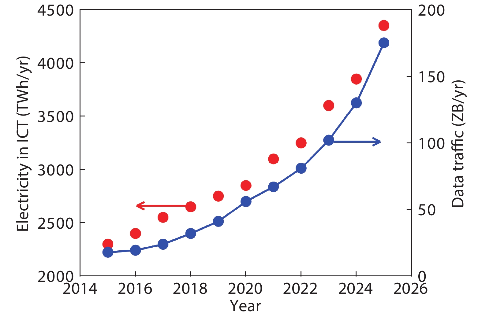
With the rapid popularization of personal computers and smartphones, the construction of 5G networks, cloud services, the Internet, and the Internet of Things, global data traffic and the consumption of information and communications technology (ICT) are explosively increasing (as shown in Fig. 1). In the short span of more than a decade in the 21st century, global data traffic has reached the ZB scale and it is predicted to continue to grow exponentially in the coming years. A recent white paper published by IDC forecasts that the global datasphere will grow up to 175ZB in 2025 from 33ZB in 2018[
![]()
Figure 1.(Color online) Forecast of global data traffic and electricity in ICT[
So far, the development of semiconductor electronic integrated circuits (IC) has basically followed Moore's Law to improve computing and storage capacity by reducing the size of transistors, optimizing the device’s structure, and increase integration. Nowadays, DCs and supercomputers use parallel operation technology: parallel processing or computing with multiple processors to improve the performance that cannot be achieved with a single processor. However, based on the existing microelectronic material system and operating principle, the transmission bandwidth of traditional copper interconnection is close to its physical limit. This makes the processing speed of chip processors much faster than the data exchange speed of the copper interconnections between the chips. Thus, the parallel processing capability between chips is restricted[
The performance of copper links in high-speed interconnection has reached its physical limit, thus a new generation of high-speed short-distance interconnection technology needs to be developed. Optical transmission has the characteristics of high bandwidth, low delay, low power consumption, low transmission loss, low crosstalk and strong spatial multiplexing capability, and has been recognized as the successor of copper links[
However, traditional photonic integrated circuit (PIC) manufacturing processes are complex because many functional photonic components are based on different material systems. For example, laser diodes (LDs) are mainly based on InP[
Silicon photonic chips have shown great potential as a new large-scale optoelectronic integrated chips because they combine low cost, large scale, high integration and reliability of mature complementary metal oxide semiconductor (CMOS) process with high bandwidth, low latency, low power consumption and strong spatial multiplexing of optical interconnects. Si is well known for its extremely low loss waveguides and various passive components, as follows:
(1) Si is a cheap and stable material. It is used to produce 300-mm large-scale wafers and the silicon-based waveguide manufacture is compatible with CMOS process. Thus, it can be integrated with CMOS electronic circuits.
(2) Si has an ultra-low material absorption coefficient at communication wavelengths.
(3) Si has an ideal oxide SiO2 with extremely low optical loss and high electrical isolation. Si waveguides have the high refractive index contrast in both horizontally and vertically on silicon-on-insulator (SOI) substrates. The curved waveguide is able to have a small radius to make the optical devices more compact and then reduce the overall PIC package area.
In addition to the monolithically integrating Si waveguides, spot-size converters (SSCs)[
However, because Si is an indirect bandgap semiconductor with low emission efficiency, it is difficult to be used as an efficient and reliable light source for silicon photonic integrated chips. Researchers proposed to dope with impurities to improve internal quantum efficiency, such as erbium doped silicon which uses Er3+ as the atomic luminescence center[
Simultaneously, it has been proposed to introduce high-gain III–V semiconductors on Si substrates to fabricate efficient LDs[
Until now, three schemes have been widely used to realize III–V high-efficiency edge emitting LDs on Si:
(1) Hybrid integration or flip-chip bonding[
(2) Heterogeneous integration or wafer-bonding[
(3) Direct hetero-epitaxial integration[
2. Silicon photonics main optical components
The overall performance improvement of a silicon photonic transceiver depends on the performance breakthrough of each optical component. The modulation speed of the active component is a main factor limiting the single-channel bandwidth. Additionally, multiplexers (MUXs) and demultiplexers (DEMUXs) also boost the total speed of a transceiver in wavelength division multiplexing (WDM). Therefore, improving the performance of silicon photonic optical components is a popular research topic for silicon photonic transceivers.
2.1. Laser diode (LD)
At present, there are three mainstream coupling methods for integrated III–V/Si lasers: 1) lens coupling[
2.1.1. Lens coupling
Luxtera's products rely on an externally packaged light source that is called the LaMP. This is a mature InP-based laser diode co-packaged with an optical isolator and a lens, as shown in Fig. 2(a)[
![]()
Figure 2.(Color online) Three coupling modes of silicon-based III–V lasers: (a) lens coupling[
2.1.2. Edge coupling
In contrast with an off-chip light source, the on-chip light source is more suitable for large-scale integration in practice situations because it does not need optical connector or introduce polarization. In Ref. [32], a 13-channel LD array is mounted on a Si waveguide platform with solder bumps by flip-chip bonding. The LD array faces the SiON waveguides facet to couple the light into them by edge coupling, as shown in Fig. 2(b). The SiON waveguides have a core section size of 2.5 × 2.5 μm2, and inversely tapered SSCs are used to transfer the optical mode into the Si optical waveguides with a core section size of 440 nm wide and 220 nm high. The alignment marks placed on the LD and the mounting stage are capable of highly accurate horizontal positioning, and the Si pedestals are also capable of highly accurate vertical positioning. An output power of up to 100 mW and good heat dissipation have been achieved by this method[
2.1.3. Evanescent coupling
Evanescent coupling avoids the alignment error by using established lithography techniques and it does not introduce SSC, which was firstly demonstrated in 2006[
2.1.4. Quantum dot laser on Si substrate
In 1982, Arakawa et al. proposed that, due to the three-dimensional quantum confinement of carriers, QD materials have a δ-function-like density of states[
![]()
Figure 3.(Color online) Comparison of typical power–current characteristics of FP lasers. QD-LD (left) is insensitive to temperature and has an almost constant threshold current and slope efficiency. Other two pictures (right two) show the characteristics of two typical QW-LDs[
Direct hetero-epitaxy of InAs/GaAs QD-LDs on Si is currently the most promising solution of monolithic integrated light sources on Si[
![]()
Figure 4.(a) TEM image of GaAs/Si interface generating a large number of dislocations[
Another advantage of QD-LDs on Si is that it has been proven to be defect-insensitive when compared to bulk material LDs and QW-LDs[
![]()
Figure 5.(Color online) (a) Schematic and TEM images of interaction between QDs and TDs[
At present, the threshold current density of the QD-LDs epitaxially grown on Si substrates can be reduced to 62.5 A/cm2, and the output power at 120 °C exceeds 105 mW[
![]()
Figure 6.(Color online) (a) Diagram of Ridge QD-LD reported by UCL university[
2.2. Modulator
In contrast from the most sensitive LiNbO3 material, monolithic integrated Si-based modulators are based on plasma free carrier effect. The refractive index of a Si waveguide changes by changing the number of free carriers by doping, electrical field methods or optical methods. Fig. 3 shows the three types of Si-based modulators: 1) PIN type, 2) PN-type and 3) MOS-type.
2.2.1. PIN type
In the ridge waveguide PIN modulator, the light field will expand into the flat plates on the two sides. Thicker plates lead to a wider pattern profile, which requires a wider p–n spacing. Thus, it will lead to large resistance, as well as low modulation efficiency and modulation rate. Because the optical modulation characteristics, such as optical mode loss, modulation efficiency, and modulation rate are very sensitive to the thickness of the Si plate, it must be made as an extremely thin when etching. To solve these difficulties, a new structure has been proposed to replace the ridge waveguide, as shown in Fig. 7(a)[
![]()
Figure 7.(Color online) Three types of silicon-based modulators: (a) PIN[
2.2.2. PN-type
The PN-type modulator increases the width of the depletion region by applying a reverse bias voltage, at the same time reduces the concentration of carriers near the PN junction. Thereby, the refractive index of the waveguide is changed and the light can be modulated. The carrier drifts extremely fast at strong electric field in the depletion region, leading in a high modulation rate. A 50 Gb/s Si modulator is shown in Fig. 7(b)[
2.2.3. MOS-type
A MOS structure modulator provides both high modulation efficiency and large modulation bandwidth. A very thin gate oxide layer is interposed between the P and N type Si of the ridge waveguide to form a capacitor structure, as shown in Fig. 7(c)[
2.3. Photodetector (PD)
Due to the inherent characteristics of the band structure, Si has low absorption coefficient and long absorption lengths in the near-infrared band, and it especially does not respond to bands above 1.1 μm. Ge material has attracted great attention to make near-infrared PDs with low dark current, high response and absorption wavelength covering 1.3–1.55 μm because Ge has a large carrier mobility and large absorption coefficient among 1.3–1.55 μm. Its band gap in the single crystal state is 0.67 eV. Additionally, because there is a thermal expansion coefficient mismatch between Ge and Si, tensile stress is introduced in Ge when it is directly grown on Si, which further narrows the Ge band gap. The absorption wavelength of Ge can be extended to 1.87 μm[
As shown in Fig. 8(a), researchers in Intel Corp. selectively deposited Ge material on a SOI substrate, which reduces the diffusion length of carriers and lowers the dislocation density[
![]()
Figure 8.(Color online) (a) Ridge waveguide PD designed by Intel Corp.[
Kotura company considers the influence of the electrode, so they reduce the width of the electrode, put the electrode away from the center of the Ge waveguide, and also increase the thickness of the Ge material[
A horizontal PIN PD with responsivity up to 1 A/W and 70 GHz bandwidth under –1 V bias has also been reported, as shown in Fig. 8(c)[
2.4. Muiltiplexer and demultiplexer
DC is used because of its ability to increase bandwidth and lower power consumption[
2.4.1. DMZI type
The multistage DMZI type (De) MUX is considered to have advantages of low insertion loss, low crosstalk, and spectral flatness. Widening the waveguide width in the DMZI region is an effective way to reduce refractive index change per unit length and keep the filter spectral wavelength nearly constant, both theoretically and experimentally[
![]()
Figure 9.(Color online) (a) Device structures of 1 × 4 Ch optical (De)MUX with different waveguide width[
2.4.2. AWG type
An AWG (De)MUX consists of two parts: two free propagation regions and an array of waveguides with successive increments in length. The spectral response of conventional AWG channel is Gaussian-like, but a flat spectral response is necessary for many WDM applications. Thus, an AWG integrated with a Multimode Interference (MMI) coupler is designed to satisfy this requirement. On SOI substrate, a high refractive index allows us to reduce the size of waveguides and are beneficial for compact design. However, it makes the design of AWG and MMI coupler difficult because the silicon waveguides are sensitive to phase error in the array. In this reference, an optimized design of compact SOI-based 12 channel 400 GHz AWG with MMI is presented[
3. Silicon photonic transceivers
Because of the rapid development of transceiver applied in DC, there has not been sufficient time to establish standards. Thus, although various solutions for short-distance optical links have been developed, they cannot interoperate. Users and customers do not need to care too much as long as the price is cheap. In this section, we introduce two solutions for short-distance optical interconnect links in DC: 1) parallel single-mode, 2) wavelength division multiplexing and two advanced modulation formats: 3) four-level pulse-amplitude modulation, and 4) coherent optical technology.
3.1. Parallel single-mode
Increasing the number of interconnect channels to increase the total bandwidth is one of the current solutions for high-speed interconnection between chips and boards. A successful PIC short-distance multi-channel interconnection solution is parallel single-mode (PSM) technology. This technology contains multiple fibers or waveguides which transmit the identical wavelength light. Small size, low power consumption, high-speed and stable interconnection thus can be achieved.
Due to their temperature-insensitive and low-RIN characteristics, as mentioned earlier, QD-LDs are very suitable as the light source on Si. High-temperature operation is essential to dense integration. The LDs can be assembled with high-temperature LSICs that generate great heat. The output power of conventional QW-LDs decreases sharply with the increase of temperature while the highest operation temperature of a QD-LD has reached 220 °C[
![]()
Figure 11.(Color online) (a) Photographs of the transmitter and receiver optical I/O core. (b) Cross section of the transmitter and receiver optical I/O core[
Researchers at AIO Core have demonstrated a fingertip-size optical module, which has received much attention in recent years[
![]()
Figure 12.(Color online) Schematic structure of a 16-channel × 25 Gb/s silicon photonic optical transceiver on a package substrate. EIC and PIC are bonded together by solder bumps and mounted on a glass ceramic interposer (GCIP)[
Fig. 12 shows a 400 G high-speed transceiver[
![]()
Figure 13.(Color online) (a) EIC and (b) PIC photographs of a high-density 16-channel optical transceiver[
Schematic diagrams of the EIC and PIC chips are shown in Fig. 13. The EIC chip and the PIC chip are directly flip-chip bonded through solder bumps to minimize the wiring length and parasitic capacitance between electronic circuits and photonic circuits. Thus, the attenuation of electrical signals between PD, driver, and modulator are reduced. At the transmitter, 2 × 8 drivers on the EIC control 2 × 8 PN-type MZI modulators on the PIC. Modulators load the electrical signals generated from pseudo random bit sequence (PRBS) on the output from hybrid integrated 4 × 4 array LDs. The light is efficiently coupled into the SSCs by passive alignment, then fed into an array of 16 GCs and finally coupled into 16 single-mode fibers. At the receiver, optical signals from 16 single-mode fibers are coupled into the PIC waveguide through 16 GCs array, and finally are sent into 4 × 4 PIN-type PD array with responsivity of 0.75 A/W at 1550 nm under –2 V reverse bias voltage. All 32 channels can transmit and receive at the same time with a modulation rate of 25 Gb/s per channel. Besides, the channel crosstalk loss is less than 0.1 dB. Therefore, the transceiver module achieved 400 Gb/s error-free (bit-error ratio (BER) < 10 –12) operation.
![]()
Figure 15.(Color online) (a) Generic transceiver architecture of the
In Ref. [57], the number of channels is increased by using beam splitters. Multiple divided channels can be modulated and overall bandwidth is improved, as shown in Fig. 14. Two groups of 13-channel array LDs are hybrid integrated on a Si substrate. 26 low optical loss “trident” SSCs, 26 1 × 4 beam splitters, 104 PIN-type modulator array, 104 inter-chip optical waveguides and 104 PIN-type PD array are monolithically integrated. Due to the modulation rate limit of the PIN-type modulator, each channel can achieve a maximum bandwidth of 20 Gb/s. Thus, transceiver of 2.1 Tb/s intra-chips interconnect has been achieved. Because the packaging area of a single channel is 0.0677 mm2, the bandwidth density reaches 30 Tbps/cm2.
![]()
Figure 17.(Color online) (a) Photograph of Sicoya’s EPIC transceiver[
A multi-source agreement (MSA) is made between multiple manufacturers to fabricate inter-compatible products for customers to choose. For example, the 100 G PSM4 is and MSA that was specifically designed for more than 500 m transmission network applications. The purpose of its formulation is to provide a low-cost solution for transmitting 4 × 25 Gbps wavelengths through SSMF outside the IEEE 100 G Ethernet specification. This 100 G PSM4 uses eight SSMFs to form four independent channels, and the speed of each channel is 25 Gb/s.
As shown in Fig. 15[
![]()
Figure 19.(Color online) (a) Top view of demultiplexer, 16-ch AWG and Ge PD array. (b) Cross section of Ge PD[
An external light source is also used in Sicoya’s design of 4 × 25 Gbit/s EPIC transceiver chip[
![]()
Figure 21.(Color online) (a) Two-bit optical DAC consisting of two EAMs. (b) Vector and eye diagram of the proposed topology optical PAM-4 generator[
A photograph of this EPIC transceiver is shown in Fig. 17(a). The RX block consists of GCs, high-efficiency Ge PDs (shown in Fig. 8(c)), TIA and limiting amplifiers. RX performance strongly benefits from the co-integration of PD and TIA, because the proximity of PD and TIA input allows a strong reduction of parasitic capacitances. Besides, elimination of transmission lines and contact pads results in much lower inductance and capacitance. At 40 Gbit/s using 215–1 not return to zero (NRZ) PRBS, an error rate of 2.5 × 10⁻¹² was obtained. At the TX, the modulation of the external laser output is achieved by a compact NMD modulator whose p–i–n diode is placed laterally to waveguide resonator[
![]()
Figure 23.(Color online) Block diagram of silicon photonic coherent PIC demonstrated by Acacia[
Commercially, Intel Corp. researchers use 4 × 25 Gb/s PSM transmission technology[
3.2. Wavelength division multiplexing
WDM is another successful short-range optical interconnect solution. Compared with PSM, WDM has the advantage of requiring only two fibers instead of N, but its disadvantage is that it requires N lasers instead of one. Compared to fiber and installation costs, WDM is more meaningful because the total cost of the transceiver is decreased.
Another MSA is 100 G CWDM4, which is a 100 G transmission solution that is based on coarse wavelength division multiplexing (CWDM). Optical signal transmission is performed by using four center wavelengths of 1270, 1290, 1310, and 1330 nm, and each wavelength transmits 25 Gb/s data. The 100 G CWDM4 module can (de)multiplex the above four center wavelength into a SSMF for transmission through CWDM technology. Intel Corp. presented a high-speed, low consumption and uncooled 4 × 25 Gb/s silicon transceiver with a CWDM wavelength interval of 20 nm in the 1310 nm band. The transmission distance is up to 10 km and it can be used in DC and 5 G front-haul[
Intel Corp. reported the first 8-channel 400 G CWDM silicon optical transmitter[
Fig. 19 shows a 16-channel WDM receiver integrated on Si[
An optical frequency comb mode-locked laser (MLL) with a wide gain spectrum can reduce the dependence of the transmitter on multiple different wavelength lasers. Therefore, the transceiver can avoid integrating multiple light sources[
Increasing the number of channels for optical communication will inevitably increase the packaging area. The advanced modulation format can increase the total bandwidth by increasing the amount of data carried per baud. Four-level pulse-amplitude modulation (PAM-4)[
3.3. Four-level pulse-amplitude modulation
The 100 Gb/s link pluggable modules in DCs (such as the PSM4 and CWDM4 mentioned above) have adopted the NRZ modulation format, which transmits single bit per baud. In comparison, each amplitude in PAM-4 transmits two bits per baud. As the interconnection rate increases from 100 to 400 Gb/s in DCs, PAM-4 direct detection format becomes the standard for DR4 and FR4 modules[
A novel compact silicon photonics transmitter that uses binary driven GeSi electro-absorption modulators (EAMs) in an interferometer topology has been demonstrated[
The pluggable QSFP28 module is based on a highly integrated silicon photonic chip and a PAM-4 ASIC[
3.4. Coherent optical technology
In contrast from short-distance transmission, which commonly adopts intensity modulation and direct detection (IMDD), coherent optical communication is required when it is applied to long-distance communication, such as interconnection between DCs, metro area network and backbone network. Because of the high cost of long-distance optical fiber, enterprises attempt to carry as much information on each optical fiber as possible. Coherent optical communication technology can load information to different characteristics of the light, such as polarization (PDM[
Acacia demonstrated a silicon-based PIC which integrated a complete vector modulator and coherent transceiver on a 2.7 × 11.5 mm2 single chip[
Researchers in Alibaba experimentally evaluated the performance of 400 G coherent and IMDD transceivers for DC optical interconnection[
4. Conclusion
For present DCs, it is technically important to increase the speed of transceivers, as well as to reduce their cost and power consumption. The optical interconnects technique is necessary for the further development of the information age, it also provides enormous bandwidth and low power consumption. Silicon photonics transceivers would take advantage of the high integration, high reliability, and low cost of the CMOS process platform to create high bandwidth, low delay, and low power consumption photonic components. The high-speed transceivers for DCs are significantly optimized in cost and performance. Optical interconnects based on VCSEL and MMF dominate short range (< 300 m) optical links thanks to their low cost, technical simplicity, and low power consumption. Edge emitting LD plays a significant role when distance beyond this range. The various LDs integration schemes have their own coupling methods. Meanwhile, due to its unique excellent characteristics, the QD-LD has shown great potential as light sources on Si, whether to adopt bonding method or monolithic integration. We believe that QD-LDs directly grown on Si would be the last piece of the puzzle of monolithic integrated silicon photonic chip. Three types of Si modulator have their own merits and drawbacks, and a suitable one can be used according to the application. Ge PD is more suitable for silicon photonics than Si, and the PIN configuration is currently the most commercially successful. Utilizing the spatial multiplexing capability of light, WDM technology further increases the transmission speed of the transceiver and a single fiber. At present, PSM and WDM technology implemented with NRZ modulation format are the mainstream in 100 G transceiver modules. Due to their ability to transmit multiple bits per baud per channel, PAM-4 modulation and coherent optical communication technology would play significant roles in 400 G and 1 TB transceiver modules in the future, as long as the performance and cost can be optimized. These transceiver modules also require their DSPs to develop better structures and algorithms to reduce the bit-error rate and the power consumption.
Acknowledgments
This work is supported by the National Key Research and Development Program of China under Grant No. 2016YFB 0402302, and the National Natural Science Foundation of China under Grant No. 91433206.
References
[1]
[2] N Jones. The information factories. Nature, 561, 163(2018).
[3] D Miller. Device requirements for optical interconnects to silicon chips. Proc IEEE, 97, 1166(2009).
[4] K Ohashi, K Nishi, T Shimizu et al. On-chip optical interconnect. Proc IEEE, 97, 1186(2009).
[5] Z G Lu, J R Liu, C Y Song et al. High performance InAs/InP quantum dot 34.462-GHz C-band coherent comb laser module. Opt Express, 26, 2160(2018).
[6] Z R Lv, Z K Zhang, X G Yang et al. Improved performance of 1.3-
[7] L Chen, Q Xu, M G Wood et al. Hybrid silicon and lithium niobate electro-optical ring modulator. Optica, 1, 112(2014).
[8] C Wang, M Zhang, X Chen et al. Integrated lithium niobate electro-optic modulators operating at CMOS-compatible voltages. Nature, 562, 101(2018).
[9] S Liao, N N Feng, D Feng. 36 GHz submicron silicon waveguide germanium photodetector. Opt Express, 19, 10967(2011).
[10] L Chen, C R Doerr, Y K Chen et al. Low-loss and broadband cantilever couplers between standard cleaved fibers and high-index-contrast Si3N4 or Si waveguides. IEEE Photonics Technol Lett, 22, 1744(2010).
[11] T Pinguet, S Denton, S Gloeckner et al. High-volume manufacturing platform for silicon photonics. Proc IEEE, 106, 2281(2018).
[12] Q Z Deng, L Liu, R Zhang et al. Athermal and flat-topped silicon Mach-Zehnder filters. Opt Express, 24, 29577(2016).
[13] T Hiraki, H Nishi, T Tsuchizawa et al. Si–Ge–silica monolithic integration platform and its application to a 22-Gb/s × 16-ch WDM receiver. IEEE Photonics J, 5, 4500407(2013).
[14] A Mekis, S Gloeckner, G Masini et al. A grating-coupler-enabled CMOS photonics platform. IEEE J Sel Top Quantum Electron, 17, 597(2011).
[15] J N Winn, D Rusin, C S Kochanek. A high-speed silicon optical modulator based on a metal-oxide-semiconducor capacitor. Nature, 427, 613(2004).
[16] C T DeRose, D C Trotter, W A Zortman et al. Ultra compact 45 GHz CMOS compatible Germanium waveguide photodiode with low dark current. Opt Express, 19, 24897(2011).
[17] H Ennen, J Schneider, G Pomrenke et al. 1.54-
[18] S Wirths, R Geiger, N von den Driesch et al. Lasing in direct-bandgap GeSn alloy grown on Si. Nat Photonics, 9, 88(2015).
[19] M d'Avezac, J W Luo, T Chanier et al. Genetic-algorithm discovery of a direct-gap and optically allowed superstructure from indirect-gap Si and Ge semiconductors. Phys Rev Lett, 108, 027401(2012).
[20] R E Camacho-Aguilera, Y Cai, N Patel et al. An electrically pumped germanium laser. Opt Express, 20, 11316(2012).
[21] Z Zhou, B Yin, J Michel. On-chip light sources for silicon photonics. Light: Sci Appl, 4, e358(2015).
[22] N Kobayashi, K Sato, M Namiwaka et al. Silicon photonic hybrid ring-filter external cavity wavelength tunable lasers. J Lightwave Technol, 33, 1241(2015).
[23] T Wang, H Liu. 1.3-
[24] S Chen, W Li, J Wu et al. Electrically pumped continuous-wave III–V quantum dot lasers on silicon. Nat Photonics, 10, 307(2016).
[25] Q Li, K W Ng, K M Lau. Growing antiphase-domain-free GaAs thin films out of highly ordered planar nanowire arrays on exact (001) silicon. Appl Phys Lett, 106, 072105(2015).
[26] C S Schulze, X Huang, C Prohl et al. Atomic structure and stoichiometry of In(Ga)As/GaAs quantum dots grown on an exact-oriented GaP/Si(001) substrate. Appl Phys Lett, 108, 143101(2016).
[27] Y Wan, Q Li, Y Geng et al. InAs/GaAs quantum dots on GaAs-on-V-grooved-Si substrate with high optical quality in the 1.3
[28] A W Fang, H Park, J E Bowers. Electrically pumped hybrid AlGaInAs–silicon evanescent laser. Opt Express, 14, 9203(2006).
[29] C Zhang, J E Bowers. Silicon photonic terabit/s network-on-chip for datacenter interconnection. Opt Fiber Technol, 44, 2(2018).
[30] E Agrell, M Karlsson, A R Chraplyvy et al. Roadmap of optical communications. J Opt, 18, 063002(2016).
[31] Y Urino, T Usuki, J Fujikata et al. High-density and wide-bandwidth optical interconnects with silicon optical interposers. Photonics Res, 2, A1(2014).
[32] T Shimizu, N Hatori, Y Arakawa. High density hybrid integrated light source with a laser diode array on a silicon optical waveguide platform for inter-chip optical interconnection. Group IV Photonics, 181(2011).
[33] B Jang, K Tanabe, S Kako et al. A hybrid silicon evanescent quantum dot laser. Appl Phys Express, 9, 092102(2016).
[34] H Wang, D Kim, M Harfouche et al. Narrow-linewidth oxide-confined heterogeneously integrated Si/III–V semiconductor lasers. IEEE Photonics Technol Lett, 29, 2199(2017).
[35] Y Arakawa, H Sakaki. Multidimensional quantum well laser and temperature dependence of its threshold current. Appl Phys Lett, 40, 939(1982).
[36] M Sugawara, M Usami. Handiling the heat QD-lasers. Nat Photonics, 3, 30(2009).
[37] K Nishi, H Saito, S Sugou et al. A narrow photoluminescence linewidth of 21 meV at 1.35
[38] K Nishi, K Takemasa, M Sugawara et al. Development of quantum dot lasers for data-com and silicon photonics applications. IEEE J Sel Top Quantum Electron, 23, 1(2017).
[39] K Takada, Y Tanaka, T Matsumoto et al. Wide-temperature-range 10.3 Gbit/s operations of 1.3
[40] A Akrout, A Shen, R Brenot et al. Separate error-free transmission of eight channels at 10 Gb/s using comb generation in a quantum-dash-based mode-locked laser. IEEE Photonics Technol Lett, 21, 1746(2009).
[41] D O'Brien, S P Hegarty, G Huyet et al. Sensitivity of quantum-dot semiconductor lasers to optical feedback. Opt Lett, 29, 1072(2004).
[42] Y G Zhou, C Zhou, C F Cao et al. Relative intensity noise of InAs quantum dot lasers epitaxially grown on Ge. Opt Express, 25, 28817(2017).
[43] M Liao, S Chen, J S Park et al. III–V quantum-dot lasers monolithically grown on silicon. Semicond Sci Technol, 33, 123002(2018).
[44]
[45] D Jung, J Norman, M J Kennedy et al. High efficiency low threshold current 1.3
[46] B Shi, L Wang, A A Taylor et al. MOCVD grown low dislocation density GaAs-on-V-groove patterned (001) Si for 1.3
[47] W Q Wei, J H Wang, B Zhang et al. InAs QDs on (111)-faceted Si (001) hollow substrates with strong emission at 1300 nm and 1550 nm. Appl Phys Lett, 113, 053107(2018).
[48] T Ward, A M Sánchez, M Tang et al. Design rules for dislocation filters. J Appl Phys, 116, 063508(2014).
[49] K Volz, A Beyer, W Witte et al. GaP-nucleation on exact Si (001) substrates for III/V device integration. J Cryst Growth, 315, 37(2011).
[50] R Alcotte, M Martin, J Moeyaert et al. Epitaxial growth of antiphase boundary free GaAs layer on 300 mm Si (001) substrate by metalorganic chemical vapour deposition with high mobility. APL Mater, 4, 046101(2016).
[51] B Zhang, W Q Wei, J H Wang et al. O-band InAs/GaAs quantum-dot microcavity laser on Si (001) hollow substrate by in-situ hybrid epitaxy. AIP Adv, 9, 015331(2019).
[52] D Jung, P G Callahan, B Shin et al. Low threading dislocation density GaAs growth on on-axis GaP/Si (001). J Appl Phys, 122, 225703(2017).
[53] A D Lee, g Q Jiang, g M C Tang et al. InAs/GaAs quantum-dot lasers monolithically grown on Si, Ge, and Ge-on-Si substrates. IEEE J Sel Top Quantum Electron, 19, 1901107(2013).
[54] M Akiyama, Y Kawarada, T Ueda et al. Growth of high quality GaAs layers on Si substrate by MOCVD. J Cryst Growth, 77, 490(1986).
[55] M Tang, S Chen, J Wu et al. 1.3-
[56] W Li, S Chen, M Tang et al. Effect of rapid thermal annealing on threading dislocation density in III–V epilayers monolithically grown on silicon. J Appl Phys, 123, 215303(2018).
[57] Y Wan, D Inoue, D Jung et al. Directly modulated quantum dot lasers on silicon with a milliampere threshold and high temperature stability. Photonics Res, 6, 776(2018).
[58] Y Urino, T Shimizu, M Okano et al. First demonstration of high density optical interconnects integrated with lasers, optical modulators and photodetectors on single silicon substrate. Opt Express, 19, B159(2011).
[59] D J Thomson, F Y Gardes, J M Fedeli et al. 50-Gb/s silicon optical modulator. IEEE Photonics Technol Lett, 24, 234(2012).
[60] J Witzens. High-speed silicon photonics modulators. Proc IEEE, 106, 2158(2018).
[61] M Ziebell, D Marris-Morini, G Rasigade et al. 40 Gbit/s low-loss silicon optical modulator based on a pipin diode. Opt Express, 20, 10591(2012).
[62] E Timurdogan, C M Sorace-Agaskar, J Sun et al. An ultralow power athermal silicon modulator. Nat Commun, 5, 4008(2014).
[63] K Debnath, D J Thomson, W Zhang et al. All-silicon carrier accumulation modulator based on a lateral metal–oxide–semiconductor capacitor. Photonics Res, 6, 373(2018).
[64] Y Ishikawa, K Wada, J Liu et al. Strain-induced enhancement of near-infrared absorption in Ge epitaxial layers grown on Si substrate. J Appl Phys, 98, 013501(2005).
[65] Y Ishikawa, K Wada, D D Cannon et al. Strain-induced band gap shrinkage in Ge grown on Si substrate. Appl Phys Lett, 82, 2044(2003).
[66] T Yin, R Cohen. 31GHz Ge n–i–p waveguide photodetectors on silicon-on-insulator substrate. Opt Express, 15, 13965(2007).
[67] G Dehlinger, S J Koester, J D Schaub et al. High-speed germanium-on-SOI lateral PIN photodiodes. IEEE Photonics Technol Lett, 16, 2547(2004).
[68] S Lischke, D Knoll, C Mai et al. High bandwidth, high responsivity waveguide-coupled germanium p–i–n photodiode. Opt Express, 23, 27213(2015).
[69] S Pathak, P Dumon, D Van Thourhout et al. Comparison of AWGs and echelle gratings for wavelength division multiplexing on silicon-on-insulator. IEEE Photonics J, 6, 1(2014).
[70] S H Jeong, Y Tanaka. Silicon-wire optical demultiplexers based on multistage delayed Mach-Zehnder interferometers for higher production yield. Appl Opt, 57, 6474(2018).
[71] S Pathak, M Vanslembrouck, P Dumon et al. Optimized silicon AWG with flattened spectral response using an MMI aperture. J Lightwave Technol, 31, 87(2013).
[72] Y Urino, N Hatori, K Mizutani et al. First demonstration of athermal silicon optical interposers with quantum dot lasers operating up to 125 °C. J Lightwave Technol, 33, 1223(2015).
[73] K Kurata, Y Suzuki, M Kurihara et al. Prospect of chip scale silicon photonics transceiver for high density multi-mode wiring system. Opt Commun, 362, 36(2016).
[74] K Yashiki, T Uemura, M Kurihara et al. 25-Gbps/ch error-free operation over 300-m MMF of low-power-consumption silicon-photonics-based chip-scale optical I/O cores. IEICE Trans Electron, E99.C, 148(2016).
[75] T Nakamura, K Yashiki, K Mizutani et al. Fingertip-size optical module, optical io core, and its application in FPGA. 2019 the Institude of Electronics, Information and Communication Engineers, E102-C, 333(2019).
[76] T Aoki, S Sekiguchi, T Simoyama et al. Low-crosstalk simultaneous 16-channel × 25 Gb/s operation of high-density silicon photonics optical transceiver. J Lightwave Technol, 36, 1262(2018).
[77]
[78]
[79] S Kupijai, H Rhee, A Al-Saadi et al. 25 Gb/s silicon photonics interconnect using a transmitter based on a node-matched-diode modulator. J Lightwave Technol, 34, 2920(2016).
[80]
[81]
[82]
[83] A Moscoso-Martir, A Tabatabaei-Mashayekh, J Muller et al. 8-channel WDM silicon photonics transceiver with SOA and semiconductor mode-locked laser. Opt Express, 26, 25446(2018).
[84] J Verbist, J Lambrecht, M Verplaetse et al. Real-time and DSP-free 128 Gb/s PAM-4 link using a binary driven silicon photonic transmitter. J Lightwave Technol, 37, 274(2019).
[85]
[86]
[87] Z Zhang, C Li, J Chen et al. Coherent transceiver operating at 61-Gbaud/s. Opt Express, 23, 18988(2015).
[88]
[89]
[90] E Depaoli, H Zhang, M Mazzini et al. A 64 Gb/s low-power transceiver for short-reach PAM-4 electrical links in 28-nm FDSOI CMOS. IEEE J Solid-State Circuits, 54, 6(2019).
[91]
[92]
[93] C R Doerr, N K Fontaine, L L Buhl. PDM-DQPSK silicon receiver with integrated monitor and minimum number of controls. IEEE Photonics Technol Lett, 24, 697(2012).
[94] D Po, L Xiang, S Chandrasekhar et al. Monolithic silicon photonic integrated circuits for compact 100+Gb/s coherent optical receivers and transmitters. IEEE J Sel Top Quantum Electron, 20, 150(2014).
[95] H Sepehrian, J Lin, L A Rusch et al. Silicon photonic IQ modulators for 400 Gb/s and beyond. J Lightwave Technol, 37, 3078(2019).
[96]


Set citation alerts for the article
Please enter your email address

© Copyright 2018-2021 | Chinese Laser Press. All Rights Reserved 沪ICP备15018463号-20