
Zhenghao Guo, Mengjun Liu, Zijia Chen, Ruizhi Yang, Peiyun Li, Haixia Da, Dong Yuan, Guofu Zhou, Lingling Shui, Huapeng Ye, "Highly efficient nonuniform finite difference method for three-dimensional electrically stimulated liquid crystal photonic devices," Photonics Res. 12, 865 (2024)
- Photonics Research
- Vol. 12, Issue 4, 865 (2024)
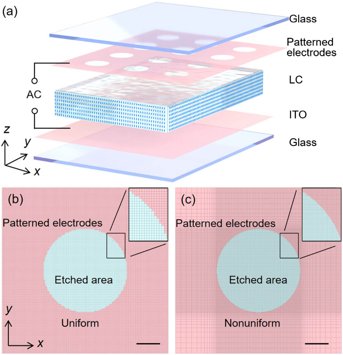
Fig. 1. (a) Schematic diagram of electrically stimulated LC photonic device. (b), (c) Grids of patterned electrode meshing in similar number of model grids. (b) Uniform grids and (c) nonuniform grids. The scale bars in (b), (c) are 10 μm.
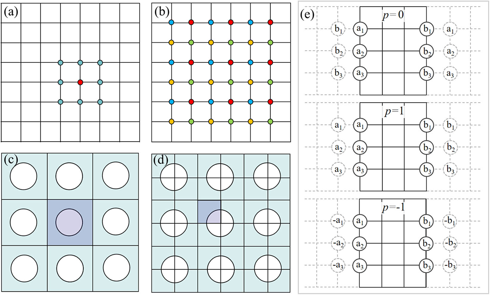
Fig. 2. (a) Schematic diagram of calculation relation. (b) Calculation sequence of SOR. (c), (d) Schematic diagram of (c) periodic and (d) symmetric boundary conditions. (e) Boundary conditions at different p
Fig. 3. (a) Schematic illustration of the unit cell of the LC photonic device. (b)–(j) Slice diagrams of the calculated tilt angle of the directors. (b)–(d) FEM, (e)–(g) uniform FDM, and (h)–(j) nonuniform FDM. (b), (e), (h) Along x x z z
Fig. 4. Comparison of mesh grid distribution between nonuniform and uniform methods. (a)–(c) Grid of nonuniform method (a) in x z x y x z x y z
Fig. 5. (a) Schematic illustration of the experimental setup to characterize the LC devices. (b), (f) Experimentally recorded light field intensity distributions at the LC layer surface of (b) array and (f) one unit. (c), (d), (e) Light field simulation results of the LC layer in the transverse plane with (c) FEM, (d) uniform FDM, and (e) nonuniform FDM. (g) Light field intensity distribution of the outermost ring of the LC layer surface in polar coordinate. (h) Simulated light field intensity distribution along the longitudinal plane. (i) Experimentally recorded light field intensity distribution along the longitudinal plane. The scale bar in (b) is 50 μm; the scale bars in (c)–(f) are 10 μm.
|
Table 1. Calculation Information of Three Methods


Set citation alerts for the article
Please enter your email address

© Copyright 2018-2021 | Chinese Laser Press. All Rights Reserved 沪ICP备15018463号-20