
Jiaqi Wei, Kumsong Kim, Fang Liu, Ping Wang, Xiantong Zheng, Zhaoying Chen, Ding Wang, Ali Imran, Xin Rong, Xuelin Yang, Fujun Xu, Jing Yang, Bo Shen, Xinqiang Wang. β-Ga2O3 thin film grown on sapphire substrate by plasma-assisted molecular beam epitaxy[J]. Journal of Semiconductors, 2019, 40(1): 012802
- Journal of Semiconductors
- Vol. 40, Issue 1, 012802 (2019)
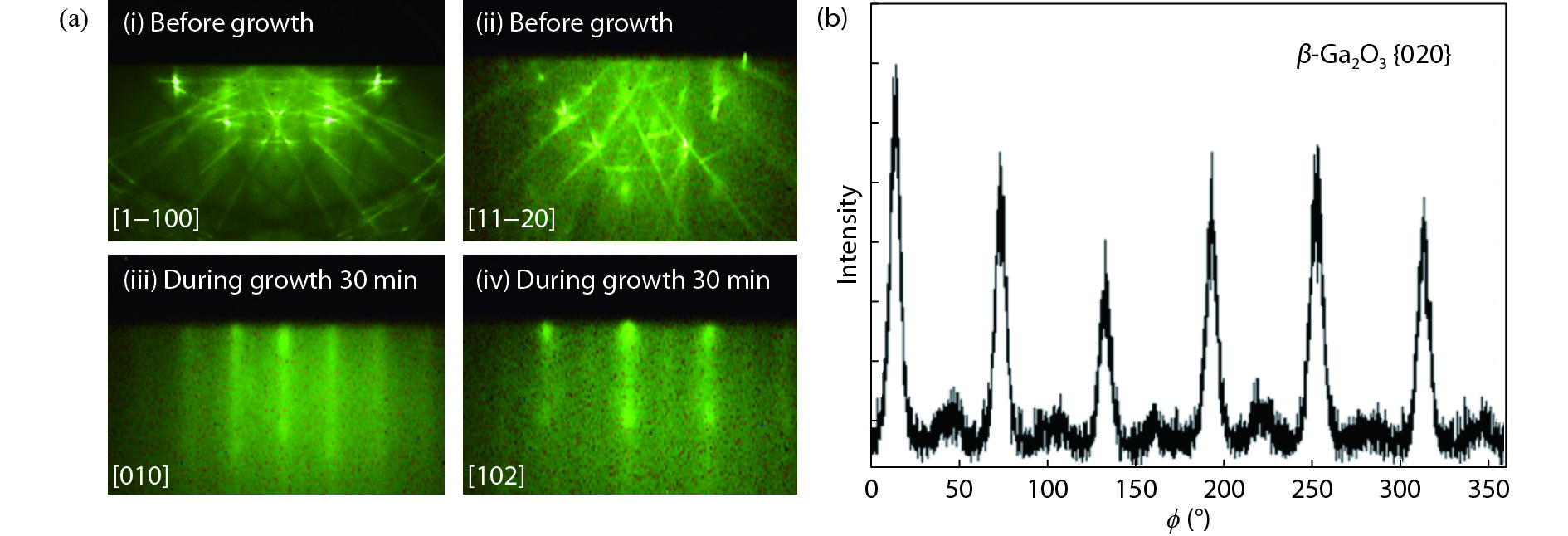
Fig. 1. (Color online) (a) RHEED patterns before and after the deposition of β -Ga2O3 films. (b) XRD in-plane ϕ scan for the β -Ga2O3 film grown at substrate temperature of 630 °C.
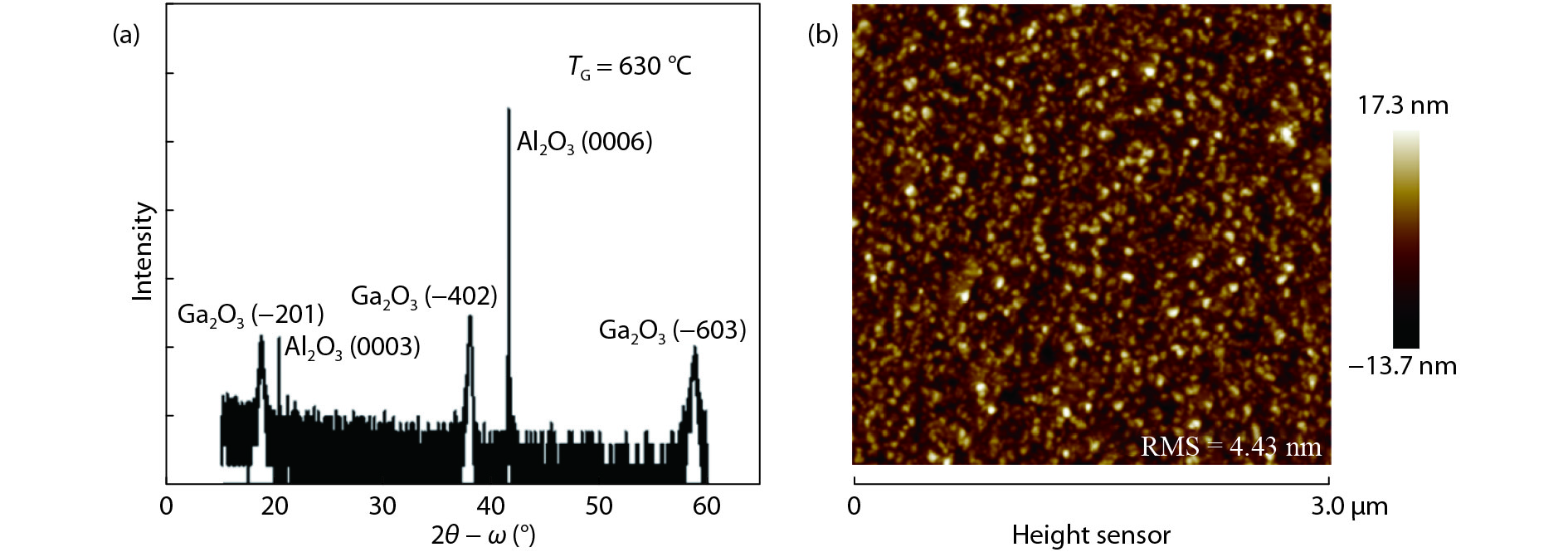
Fig. 2. (Color online) (a) XRD 2θ –ω scan of Ga2O3/ Al2O3 grown at 630 °C. (b) Surface morphology investigated by AFM in a scanned area of 3 × 3 μ m2.
Fig. 3. (Color online) A growth diagram for the Ga2O3 MBE growth. The Ga flux dependent growth rate of Ga2O3 grown at different temperatures.
Fig. 4. (Color online) (a) XRD patterns of Ga2O3 films deposited on (0001) sapphire substrates with different substrate temperatures. (b) The growth temperature dependent FWHM of XRD ω -scan for (
Fig. 5. (Color online) AFM surface morphology of β -Ga2O3 deposited at different substrate temperatures. (a) 630 °C. (b) 680 °C. (c) 730 °C. (d) 780 °C.
Fig. 6. (Color online) RT-CL spectra of (a) 400-nm-thick β -Ga2O3 film, (b) cross sectional β -Ga2O3 thin film, (c) Al2O3 substrate.

Set citation alerts for the article
Please enter your email address
© Copyright 2018-2021 | Chinese Laser Press. All Rights Reserved 沪ICP备15018463号-20