• Journal of Semiconductors
  • Vol. 40, Issue 1, 012802 (2019)
Jiaqi Wei, Kumsong Kim, Fang Liu, Ping Wang, Xiantong Zheng, Zhaoying Chen, Ding Wang, Ali Imran, Xin Rong, Xuelin Yang, Fujun Xu, Jing Yang, Bo Shen, and Xinqiang Wang
Author Affiliations
  • State Key Laboratory of Artificial Microstructure and Mesoscopic Physics, School of Physics, Peking University, Beijing 100871, China
  • show less
    DOI: 10.1088/1674-4926/40/1/012802 Cite this Article
    Jiaqi Wei, Kumsong Kim, Fang Liu, Ping Wang, Xiantong Zheng, Zhaoying Chen, Ding Wang, Ali Imran, Xin Rong, Xuelin Yang, Fujun Xu, Jing Yang, Bo Shen, Xinqiang Wang. β-Ga2O3 thin film grown on sapphire substrate by plasma-assisted molecular beam epitaxy[J]. Journal of Semiconductors, 2019, 40(1): 012802 Copy Citation Text show less

    Abstract

    Monoclinic gallium oxide (Ga2O3) has been grown on (0001) sapphire (Al2O3) substrate by plasma-assisted molecular beam epitaxy (PA-MBE). The epitaxial relationship has been confirmed to be [010]( ) β-Ga2O3||[ ](0001)Al2O3 via in-situ reflection high energy electron diffraction (RHEED) monitoring and ex-situ X-ray diffraction (XRD) measurement. Crystalline quality is improved and surface becomes flatter with increasing growth temperature, with a best full width at half maximum (FWHM) of XRD ω-rocking curve of ( ) plane and root mean square (RMS) roughness of 0.68° and 2.04 nm for the sample grown at 730 °C, respectively. Room temperature cathodoluminescence measurement shows an emission at ~417 nm, which is most likely originated from recombination of donor–acceptor pair (DAP).

    1. Introduction

    β-Ga2O3, a semiconductor with a bandgap energy of 4.6–4.9 eV at 300 K[1, 2], exhibits a great breakdown electric field of 6–8 MV/cm[3, 4] and high transparency in the deep ultraviolet (UV) and visible wavelength region. Therefore, β-Ga2O3 is attracting interest for solar-blind UV photodetectors[1, 5], gas sensors[6], transparent conducting films for electrodes on a variety of Schottky barrier diode (SBD)[4, 7, 8], metal–semiconductor field effect transistors (MESFETs)[9], metal oxide semiconductor field-effect transistors (MOSFETs)[4, 9], high dielectric oxide or active material for FET device and so on[1012]. Another important feature of Ga2O3 is that its substrate can be fabricated at low cost from bulk single crystal using the same methods such as floating zone (FZ)[13] and the edge-defined film-fed growth (EFG)[2, 14, 15] employed for manufacturing sapphire substrate, which provides a potential in mass production at low cost.

    Many techniques have been employed to prepare Ga2O3 thin films, including sol-gel methods[16, 17], magnetron sputtering[18, 19], metal-organic chemical vapor deposition (MOCVD)[2022], pulsed laser deposition (PLD)[2325] and molecular beam epitaxy[2628]. Among them, MBE is an ideal technology for the growth of high quality and high purity Ga2O3 thin films due to ultrahigh vacuum growth environment and precise controllability on the growth parameters, though the growth rate is lower than some other growth methods such as MOCVD[22]. However, it is still a challenge to grow high quality β-Ga2O3 thin film on sapphire substrate, due to the large lattice mismatch between the β-Ga2O3 and sapphire.

    In this paper, we report the systematical study on growth of β-Ga2O3 thin film on (0001) Al2O3 substrate by PA-MBE. It was found that crystal quality and surface flatness were improved with increasing growth temperature up to 730 °C, with a best full width at half maximum (FWHM) of XRD ω-rocking curve of ( ) plane and root mean square (RMS) roughness of 0.68° and 2.04 nm, respectively. Room temperature cathodoluminescence measurement shows an emission at ~417 nm, which is most likely originated from the recombination of acceptor or donor–acceptor pair (DAP).

    2. Experimental methods

    Ga2O3 thin films are grown on (0001) plane sapphire substrate by PREVAC PA-MBE. The Ga beam is supplied by a conventional Knudsen-cell and the flux is modified by the temperature of Ga-cell. O atoms are supplied by a radio frequency plasma cell for oxygen gas, with a constant oxygen flux of 2 sccm and a forward plasma power of 280 W. The typical growth time is 200 min for all films. Reflection high-energy electron diffraction (RHEED) was used to monitor the growth process. The crystal structure and surface morphology were analyzed by X-ray diffraction (XRD), scanning electron microcopy (SEM) and atomic force microscopy (AFM). Cathodoluminescence (CL) measurement was performed at room temperature to characterize emission of the Ga2O3 thin films.

    3. Results and discussion

    3.1. Structural characterization

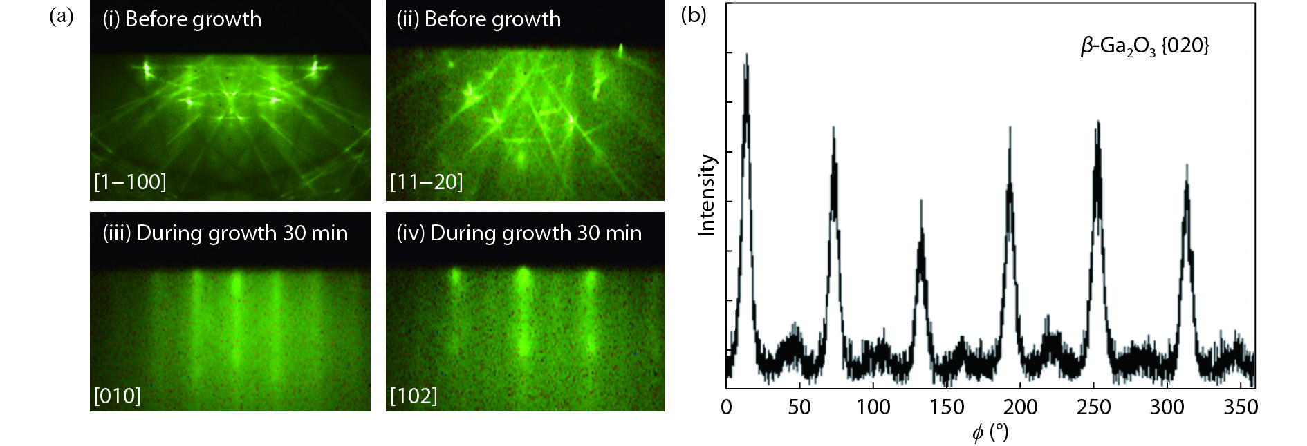
    The whole growth procedure was in-situ monitored by RHEED. Fig. 1(a) shows the evolution of RHEED patterns before and after the deposition of Ga2O3 and displays that the films are single crystal. The typical RHEED patterns of sapphire (0001) plane along [ ] and [ ] azimuths were clearly observed before the growth of Ga2O3. As soon as the deposition of Ga2O3 starts, the bright fringes of sapphire were gradually transformed into faint streaky patterns. Fig. 1(a) (iii) and (iv) exhibit the RHEED patterns of Ga2O3 recorded at the same electron injection directions as those in Fig. 1(a) (i) and (ii), respectively. Compared with the patterns from sapphire substrate, not only the pattern intensity dimmed, but also the fringe spacing changed, indicating that new crystal structure is appeared. Taking into account the rectangle arranged in-plane atoms, one can easily predict that the RHEED patterns shown in Fig. 1(a) (iii) and (iv) were collected along the [010] and [102] azimuth ofβ-Ga2O3, respectively. And the epitaxial relationship between sapphire and Ga2O3 should be [010]( )β-Ga2O3||[ ](0001)Al2O3 and [102]( )β-Ga2O3||[ ](0001)Al2O3 with the lattice mismatch value of 4.2% and 10.7%, respectively[10, 22].

    (Color online) (a) RHEED patterns before and after the deposition of β-Ga2O3 films. (b) XRD in-plane ϕ scan for the β-Ga2O3 film grown at substrate temperature of 630 °C.

    Figure 1.(Color online) (a) RHEED patterns before and after the deposition of β-Ga2O3 films. (b) XRD in-plane ϕ scan for the β-Ga2O3 film grown at substrate temperature of 630 °C.

    Meanwhile, the RHEED patterns were observed periodically every 60° rotation starting at the [ ] azimuth of Al2O3, which agrees well with the in-plane XRD scan result for the film grown at 630 °C shown in Fig. 1(b). The six peaks that appear every 60° indicate 6-fold in-plane rotational symmetry. Considering the fact that monoclinic β-Ga2O3 { } planes originally have 2-fold in-plane rotational symmetry, it can be concluded that the grown film contains in-plane rotational domains. The appearance of rotational domains is due to the 3-fold rotational symmetry of the c-sapphire surface; that is, the originally 2-fold β-Ga2O3 epitaxially grew in the three different directions at same rates, resulting in the 6-fold rotational symmetry[26, 29].

    Fig. 2(a) presents the XRD 2θ–ω scan of the Ga2O3/Al2O3 sample grown at 630 °C. Comparing with the standard PDF card (No.: 43-1012)[29], the three diffraction peaks located at 18.98°, 38.48° and 59.28° can be ascribed to ( ), ( ), and ( ) planes of β-Ga2O3, respectively[3032]. The result indicates that the film deposited on (0001) Al2O3 substrate is pure β-Ga2O3 with single orientation along the [ ] direction and further confirms the predicted epitaxy relationship from the RHEED patterns.

    FWHM of the XRD rocking curve obtained from the diffraction peak of ( ) plane was used to represent the crystal quality. The FWHM of ( ) of this sample is about 1.45°. According to the 3 × 3 μm2 AFM image shown in Fig. 2(b), the corresponding RMS roughness is about 4.43 nm, indicating that the crystalline quality is not satisfied. In order to improve the crystal quality and surface flatness of Ga2O3 epilayer, the growth conditions need to be optimized.

    3.2. Growth conditions optimization

    To optimize the efficient Ga to O atoms ratio, the growth temperature was maintained at 630 °C where the desorption of Ga adatoms nearly negligible, while the oxygen flux was kept constant at 2 sccm with forward plasma power of 280 W. The thickness of the β-Ga2O3 film was obtained by fitting the X-ray reflectivity (XRR) curve and further verified by scanning electron microscope (SEM) measurement. Even though the growth rate of β-Ga2O3 is low, it is clearly observed from the growth diagram shown in Fig. 3 that the growth rate increases almost linearly with increasing Ga flux up to 1.0 × 10⁻⁶ mbar at a fixed growth temperature of 630 °C and then the growth rate tends to decrease in the higher Ga flux. During the growth of Ga2O3, there is a competition between Ga2O3 (epilayer) and Ga2O (gas). The reactions for the layer growth and suboxide formations are[33]:

    $ 2{\rm{Ga}}\left( {\rm{g}} \right) + 3{\rm{O}}\left( {\rm{g}} \right) \to {\rm{G}}{{\rm{a}}_2}{{\rm{O}}_3}\left( {\rm{s}} \right){\rm{ }}, $  (1)

    $ 2{\rm{Ga}}\left( {\rm{g}} \right) + 1{\rm{O}}\left( {\rm{g}} \right) \to {\rm{G}}{{\rm{a}}_2}{{\rm{O}}_1}\left( {\rm{g}} \right){\rm{ }}. $  (2)

    The labels g and s denote the gas and solid phase, respectively. The redundant Ga and O adatoms will form Ga2O, then desorb from the surface and does not contribute to the epitaxy of Ga2O3. This tendency has also been observed in other groups[26, 33], indicating that the growth rate is limited by the minority atom species on the growing surface and therefore the behavior in Fig. 3 can be classified into two regions of O-rich and Ga-rich. Since in Ref. [34], the growth around the stoichiometric region has resulted in the best quality, the optimum Ga flux was taken to be 1.0 × 10⁻⁶ mbar.

    (Color online) (a) XRD 2θ–ω scan of Ga2O3/ Al2O3 grown at 630 °C. (b) Surface morphology investigated by AFM in a scanned area of 3 × 3 μm2.

    Figure 2.(Color online) (a) XRD 2θ–ω scan of Ga2O3/ Al2O3 grown at 630 °C. (b) Surface morphology investigated by AFM in a scanned area of 3 × 3 μm2.

    To explore the influence of growth temperature, several samples were grown at different temperatures ranging from 630 to 830 °C and the efficient Ga/O flux ratio was set at stoichiometric region. The XRD 2θ–ω scan spectra are presented in Fig. 4, Three diffraction peaks are observed in addition to the substrate’s peaks at 630 °C, 680 °C and 730 °C, which can be ascribed to the diffraction peaks from ( ), ( ) and ( ) planes of β-Ga2O3 with single orientation along the [ ] direction. Surprisingly, both of the ( ) and ( ) diffraction peaks of β-Ga2O3 disappear when the growth temperature is above 730 °C, and only the ( ) peak survives but tends to be annihilated. The absence of ( ) and ( ) peaks and the faint ( ) peak indicate the degradation of crystal structure and the reduction of growth rate due to the relatively large decomposition rate at higher growth temperature region. At higher temperature (780 °C and 830 °C), the stress caused by different coefficients of thermal expansion between film and substrate destroys the epitaxial growth, and the structure of the film changes to somehow polycrystalline[22]. The results imply that the film grown at 730 °C has optimized crystallization with an out-plane relationship of β-Ga2O3( )||Al2O3(0001).

    Luckily, all of the diffraction peaks from β-Ga2O3 completely existed at lower growth temperature region (630–730 °C). Besides, the XRD peak intensity gradually increase and the line width gradually decrease with increasing growth temperature, indicating the improvement of crystal quality.

    Fig. 4(b) shows FWHM of XRD ω-rocking curve for ( ) plane of β-Ga2O3 layers grown at different temperatures. Apparently, the FWHM value monotonically decreases with increasing growth temperature, and the values are 1.45°, 0.82°, and 0.68° for 630, 680, and 730 °C, respectively. The improvement of crystal quality with increasing growth temperature is a common phenomenon for materials epitaxy, but limited up to 730 °C for β-Ga2O3 in our MBE system.

    (Color online) A growth diagram for the Ga2O3 MBE growth. The Ga flux dependent growth rate of Ga2O3 grown at different temperatures.

    Figure 3.(Color online) A growth diagram for the Ga2O3 MBE growth. The Ga flux dependent growth rate of Ga2O3 grown at different temperatures.

    Fig. 5 shows surface morphology of Ga2O3 grown at different temperatures. Clearly, with increasing growth temperature, the RMS roughness in a scanned area of 3 × 3 μm2 gradually decreases from 4.43 nm (630 °C) to 1.32 nm (780 °C). Therefore, higher growth temperature is beneficial to improve surface flatness. Taking into account the AFM image shown in Fig. 2(b) (grown at 630 °C), all of the Ga2O3 surfaces were covered with crystal grains rather than steps. The large lattice mismatch (4.2% and 10.7%) between Ga2O3 and sapphire should be responsible for this phenomenon. Statistical analysis shows that the grain size significantly decreases with increasing growth temperature, while the grain density changes to the opposite direction. The evolution of grain size and density mainly result from the enhancement of adatoms diffusion length and the reduction of critical nucleation size with increasing growth temperature. Considering the growth rate, crystal quality, and surface flatness, the optimized growth temperature in our MBE system is 730 °C, and the corresponding Ga2O3 epilayer exhibits a FWHM of ( ) about 0.68° with a RMS value ~2.04 nm.

    (Color online) (a) XRD patterns of Ga2O3 films deposited on (0001) sapphire substrates with different substrate temperatures. (b) The growth temperature dependent FWHM of XRD ω-scan for () plane of Ga2O3 films.

    Figure 4.(Color online) (a) XRD patterns of Ga2O3 films deposited on (0001) sapphire substrates with different substrate temperatures. (b) The growth temperature dependent FWHM of XRD ω-scan for ( ) plane of Ga2O3 films.

    (Color online) AFM surface morphology of β-Ga2O3 deposited at different substrate temperatures. (a) 630 °C. (b) 680 °C. (c) 730 °C. (d) 780 °C.

    Figure 5.(Color online) AFM surface morphology of β-Ga2O3 deposited at different substrate temperatures. (a) 630 °C. (b) 680 °C. (c) 730 °C. (d) 780 °C.

    3.3. Optical characterization

    Room temperature cathodeluminescence (RT-CL) have been performed on the surface and cross section of Ga2O3/Al2O3 and Al2O3 substrate. The spectra in Fig. 6 shows a strong broad UV-blue and a weak red emission band centered at 325, 417 and 650 nm. Unfortunately, we did not find any band edge emission (240–270 nm) from these samples. Comparing with the emission behavior of sapphire substrate shown in Fig. 6(c), the emission peak in Fig. 6(b) around 325 and 650 nm mainly results from the defects in sapphire while the emission with peak at 417 nm comes from β-Ga2O3 film. This blue emission is due to recombination of electron on donor and hole at acceptor or donor–acceptor pair (DAP). These donors might be dominated by oxygen vacancies (VO) and acceptors might be created by gallium vacancies (VGa) or gallium–oxygen vacancies pair (VGa–VO)[3537]. It is clear that the quality of β-Ga2O3 film is not good enough and further study should be done to improve it.

    (Color online) RT-CL spectra of (a) 400-nm-thick β-Ga2O3 film, (b) cross sectional β-Ga2O3 thin film, (c) Al2O3 substrate.

    Figure 6.(Color online) RT-CL spectra of (a) 400-nm-thick β-Ga2O3 film, (b) cross sectional β-Ga2O3 thin film, (c) Al2O3 substrate.

    4. Conclusions

    In conclusion, β-Ga2O3 thin film has been grown on (0001) sapphire substrate by PA-MBE, and the epitaxial relationship is confirmed as [010]( )β-Ga2O3||[ ](0001)Al2O3. Crystalline quality and surface flatness have been improved with increasing growth temperature with the best FWHM of XRD ω-scans of ( ) plane and RMS roughness of 0.68° and 2.04 nm, respectively. RT-CL spectra suggests that the β-Ga2O3 thin film exhibits a strong defects-related emission at around 417 nm and further improvement of crystalline quality is needed.

    Acknowledgements

    This work was supported by the National Key R&D Program of China (No. 2018YFB0406502) and the National Natural Science Foundation of China (Nos. 61734001, 61521004).

    References

    [1] D Guo, Z Wu, P Li et al. Fabrication of β-Ga2O3 thin films and solar-blind photodetectors by laser MBE technology. Opt Mater Express, 4, 1067(2014).

    [2] W Mu, Z Jia, Y Yin et al. High quality crystal growth and anisotropic physical characterization of β-Ga2O3 single crystals grown by EFG method. J Alloys Compd, 714, 453(2017).

    [3] S J Pearton, J Yang, C Patrick et al. A review of Ga2O3 materials, processing, and devices. Appl Phys Rev, 5, 011301(2018).

    [4] H Xue, Q He, G Jian et al. An overview of the ultrawide bandgap Ga2O3 semiconductor-based schottky barrier diode for power electronics application. Nanoscale Res Lett, 13, 290(2018).

    [5] X Zhao, W Cui, Z Wu et al. Growth and characterization of Sn doped β-Ga2O3 thin films and enhanced performance in a solar-blind photodetector. J Electron Mater, 46, 2366(2017).

    [6] S S Kumar, E J Rubio, M Noor-A-Alam et al. Structure, morphology, and optical properties of amorphous and nanocrystalline gallium oxide thin films. J Phys Chem C, 117, 4194(2013).

    [7] E Farzana, E Ahmadi, J S Speck et al. Deep level defects in Ge-doped (010) β-Ga2O3 layers grown by plasma-assisted molecular beam epitaxy. J Appl Phys, 123, 1(2018).

    [8] Z Hu, H Zhou, Q Feng et al. Field-plated lateral β-Ga2O3 schottky barrier diode with high reverse blocking voltage of more than 3 kV and high DC power figure-of-merit of 500 MW/cm2. IEEE Electron Device Lett, 39, 1564(2018).

    [9] M Higashiwaki, K Sasaki, A Kuramata et al. Development of gallium oxide power devices. Phys Status Solidi, 211, 21(2014).

    [10] Z Galazka. β-Ga2O3 for wide-bandgap electronics and optoelectronics. Semicond Sci Technol, 33, 113001(2018).

    [11] S Kumar, C Tessarek, S Christiansen et al. A comparative study of β-Ga2O3 nanowires grown on different substrates using CVD technique. J Alloys Compd, 587, 812(2014).

    [12] S Rafique, L Han, A T Neal et al. Towards high mobility heteroepitaxial β-Ga2O3 on sapphire-dependence on the substrate off-axis angle. Phys Status Solidi, 215, 1700467(2018).

    [13] E G Víllora, K Shimamura, Y Yoshikawa et al. Large-size β-Ga2O3 single crystals and wafers. J Cryst Growth, 270, 420(2004).

    [14] H Aida, K Nishiguchi, H Takeda et al. Growth of β-Ga2O3 single crystals by the edge-defined, film fed growth method. Jpn J Appl Phys, 47, 8506(2008).

    [15] M Higashiwaki, K Konishi, K Sasaki et al. Temperature-dependent capacitance–voltage and current-voltage characteristics of Pt/Ga2O3 (001) Schottky barrier diodes fabricated on n-Ga2O3 drift layers grown by halide vapor phase epitaxy. Appl Phys Lett, 108, 133503(2016).

    [16] G Sinha, K Adhikar, S Chaudhuri et al. Sol-gel derived phase pure α-Ga2O3 nanocrystalline thin film and its optical properties. J Cryst Growth, 276, 204(2005).

    [17] Y Kokubun, K Miura, F Endo et al. Sol-gel prepared β-Ga2O3 thin films for ultraviolet photodetectors. Appl Phys Lett, 90, A316(2007).

    [18] M Fleischer, W Hanrieder, H Meixner. Stability of semiconducting gallium oxide thin films. Thin Solid Films, 190, 93(1990).

    [19] J J Liu, J L Yan, L Shi et al. Electrical and optical properties of deep ultraviolet transparent conductive Ga2O3/ITO films by magnetron sputtering. J Semicond, 31, 103001(2010).

    [20] Z Ji, J Du, J Fan et al. Gallium oxide films for filter and solar-blind UV detector. Opt Mater, 28, 415(2006).

    [21] M Fleischer, W Hanrieder, H Meixner. Stability of semiconducting gallium oxide thin films. Thin Solid Films, 190, 93(2015).

    [22] Y Lv, J Ma, W Mi et al. Characterization of β-Ga2O3 thin films on sapphire (0001) using metal-organic chemical vapor deposition technique. Vacuum, 86, 1850(2012).

    [23] H Hayashi, R Huang, F Oba et al. Epitaxial growth of Mn-doped γ-Ga2O3 on spinel substrate. J Mater Res, 26, 578(2011).

    [24] K Matsuzaki, H Hiramatsu, K Nomura et al. Growth, structure and carrier transport properties of Ga2O3 epitaxial film examined for transparent field-effect transistor. Thin Solid Films, 496, 37(2006).

    [25] F Zhang, K Saito, T Tanaka et al. Electrical properties of Si doped Ga2O3 films grown by pulsed laser deposition. J Mater Sci: Mater Electron, 26, 9624(2015).

    [26] T Oshima, T Okuno, S Fujita. Ga2O3 thin film growth on C-plane sapphire substrates by molecular beam epitaxy for deep-ultraviolet photodetectors. Jpn J Appl Phys, 46, 7217(2007).

    [27] S Nakagomi, Y Kokubun. Crystal orientation of β-Ga2O3 thin films formed on C-plane and A-plane sapphire substrate. J Cryst Growth, 349, 12(2012).

    [28] Y Zhang, C Joishi, Z Xia et al. Demonstration of β-(AlxGa1−x)2O3/Ga2O3 double heterostructure field effect transistors. Appl Phys Lett, 112, 233503(2018).

    [29] F B Zhang, K Saito, T Tanaka et al. Structural and optical properties of Ga2O3, films on sapphire substrates by pulsed laser deposition. J Cryst Growth, 387, 96(2014).

    [30] L Huang, Q Feng, G Han et al. Comparison study of β-Ga2O3 photodetectors grown on sapphire at different oxygen pressures. IEEE Photonics J, 9, 1(2017).

    [31] Z Cheng, M Hanke, P Vogt et al. Phase formation and strain relaxation of Ga2O3 on C-plane and A-plane sapphire substrates as studied by synchrotron-based x-ray diffraction. Appl Phys Lett, 111, 162104(2017).

    [32] E G Villora, K Shimamura, K Kitamura et al. Rf-plasma-assisted molecular-beam epitaxy of β-Ga2O3. Appl Phys Lett, 88, 841(2006).

    [33] P Vogt, O Bierwagen. Reaction kinetics and growth window for plasma-assisted molecular beam epitaxy of Ga2O3: Incorporation of Ga vs. Ga2O desorption. Appl Phys Lett, 108, 024001(2016).

    [34] P Ravadgar, R H Horng, S D Yao et al. Effects of crystallinity and point defects on optoelectronic applications of β-Ga2O3 epilayers. Opt Express, 21, 24599(2013).

    [35] G Guzmán-Navarro, M Herrera-Zaldívar, J Valenzuela-Benavides et al. CL study of blue and UV emissions in β-Ga2O3 nanowires grown by thermal evaporation of GaN. J Appl Phys, 110, 033517(2011).

    [36] D P Yu, J L Bubendorff, J F Zhou et al. Localized cathodoluminescence investigation on single Ga2O3 nanoribbon/nanowire. Solid State Commun, 124, 417(2002).

    [37] J Hao, M Cocivera. Optical and luminescent properties of undoped and rare-earth-doped Ga2O3 thin films deposited by spray pyrolysis. J Phys D Appl Phys, 35, 433(2002).

    Jiaqi Wei, Kumsong Kim, Fang Liu, Ping Wang, Xiantong Zheng, Zhaoying Chen, Ding Wang, Ali Imran, Xin Rong, Xuelin Yang, Fujun Xu, Jing Yang, Bo Shen, Xinqiang Wang. β-Ga2O3 thin film grown on sapphire substrate by plasma-assisted molecular beam epitaxy[J]. Journal of Semiconductors, 2019, 40(1): 012802
    Download Citation