• Photonics Research
  • Vol. 9, Issue 9, 1650 (2021)
Rui Feng1、2, Badreddine Ratni3, Jianjia Yi4、6, Hailin Zhang1, André de Lustrac2、5, and Shah Nawaz Burokur3、*
Author Affiliations
  • 1Key Laboratory of Integrated Services Networks, Xidian University, Xi’an 710071, China
  • 2Université Paris-Saclay, CNRS, Centre de Nanosciences et de Nanotechnologies, 91120 Palaiseau, France
  • 3LEME, UPL, Univ Paris Nanterre, F92410 Ville d’Avray, France
  • 4School of Information and Communications Engineering, Xi’an Jiaotong University, Xi’an 710049, China
  • 5UPL, Univ Paris Nanterre, F92410 Ville d’Avray, France
  • 6e-mail: jianjia.yi@xjtu.edu.cn
  • show less
    DOI: 10.1364/PRJ.428853 Cite this Article Set citation alerts
    Rui Feng, Badreddine Ratni, Jianjia Yi, Hailin Zhang, André de Lustrac, Shah Nawaz Burokur. Versatile metasurface platform for electromagnetic wave tailoring[J]. Photonics Research, 2021, 9(9): 1650 Copy Citation Text show less
    Schematic of complex beams generation exploiting the versatile metasurface platform. Three complex beams, including zeroth-order Bessel beam, vortex beam, and Airy beam, are generated by judiciously implementing the predefined phase profiles.
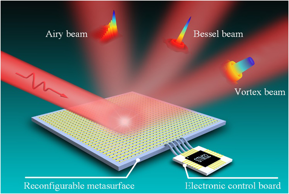
    Fig. 1. Schematic of complex beams generation exploiting the versatile metasurface platform. Three complex beams, including zeroth-order Bessel beam, vortex beam, and Airy beam, are generated by judiciously implementing the predefined phase profiles.
    Schematic design of the addressable meta-atom incorporating a voltage-biased varactor diode. (a) 3D view. The inset shows the equivalent circuit of the meta-atom. (b) Exploded perspective view. The geometrical parameters are p=6 mm, w1=1.1 mm, w2=0.25 mm, w3=0.16 mm, g1=3.6 mm, g2=0.205 mm, l=5.8 mm, q1=0.73 mm, and q2=0.6 mm. (c)–(f) Reflection magnitude and phase responses of the meta-atom for different stimuli signals in the frequency band ranging from 7 to 11 GHz obtained from (c), (d) numerical simulations and (e), (f) experimental characterizations.
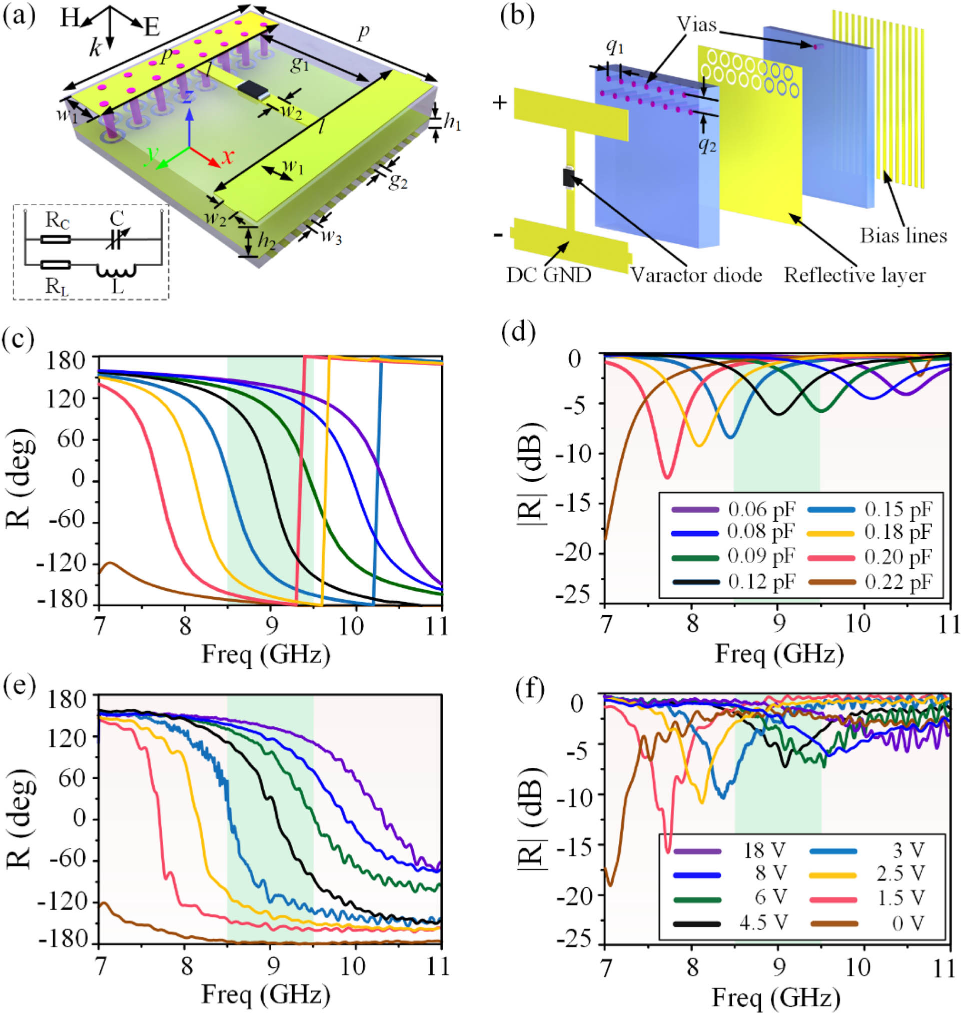
    Fig. 2. Schematic design of the addressable meta-atom incorporating a voltage-biased varactor diode. (a) 3D view. The inset shows the equivalent circuit of the meta-atom. (b) Exploded perspective view. The geometrical parameters are p=6  mm, w1=1.1  mm, w2=0.25  mm, w3=0.16  mm, g1=3.6  mm, g2=0.205  mm, l=5.8  mm, q1=0.73  mm, and q2=0.6  mm. (c)–(f) Reflection magnitude and phase responses of the meta-atom for different stimuli signals in the frequency band ranging from 7 to 11 GHz obtained from (c), (d) numerical simulations and (e), (f) experimental characterizations.
    Reflection response of the meta-atom versus the position variation y1 of the through via for four different capacitance values at 9 GHz. (a) Phase without blind vias. (b) Phase with blind vias. (c) Magnitude without blind vias. (d) Magnitude with blind vias. The use of blind vias allows achieving a stable reflection response independent of the location of the meta-atom on the metasurface.
    Fig. 3. Reflection response of the meta-atom versus the position variation y1 of the through via for four different capacitance values at 9 GHz. (a) Phase without blind vias. (b) Phase with blind vias. (c) Magnitude without blind vias. (d) Magnitude with blind vias. The use of blind vias allows achieving a stable reflection response independent of the location of the meta-atom on the metasurface.
    Photographs of the dynamic metasurface. (a) Top face of the fabricated sample. Ultrathin absorbing sheets, represented by the gray material, are placed around the usable surface to eliminate parasitic reflections. (b) Bottom face of the sample containing the bias lines and flexible printed circuit (FPC) connectors. (c) Usable part of the metasurface whose size is 180 mm×180 mm. (d) Zoomed detail of the metasurface showing the varactor-loaded meta-atom.
    Fig. 4. Photographs of the dynamic metasurface. (a) Top face of the fabricated sample. Ultrathin absorbing sheets, represented by the gray material, are placed around the usable surface to eliminate parasitic reflections. (b) Bottom face of the sample containing the bias lines and flexible printed circuit (FPC) connectors. (c) Usable part of the metasurface whose size is 180  mm×180  mm. (d) Zoomed detail of the metasurface showing the varactor-loaded meta-atom.
    (a)–(c) Phase profiles for the zeroth-order Bessel beam generation at 8.5, 9, and 9.5 GHz. (d)–(k) Numerical and experimental results of the zeroth-order Bessel beam at 8.5, 9, and 9.5 GHz. (d)–(f) Simulated electric field magnitude distributions in xoz and yoz planes, where the subfigures show the magnitude and phase distributions in the xoy transverse plane at z=15 cm. (g)–(i) Corresponding experimental near-field mappings. (j), (k) Normalized far-field patterns in both xoz and yoz planes at 9.5 GHz.
    Fig. 5. (a)–(c) Phase profiles for the zeroth-order Bessel beam generation at 8.5, 9, and 9.5 GHz. (d)–(k) Numerical and experimental results of the zeroth-order Bessel beam at 8.5, 9, and 9.5 GHz. (d)–(f) Simulated electric field magnitude distributions in xoz and yoz planes, where the subfigures show the magnitude and phase distributions in the xoy transverse plane at z=15  cm. (g)–(i) Corresponding experimental near-field mappings. (j), (k) Normalized far-field patterns in both xoz and yoz planes at 9.5 GHz.
    (a)–(c) Phase profiles for the generation of different types of vortex beams carrying OAM mode l=1 at 9.5 GHz. (d)–(k) Numerical and experimental results of different types of vortex beams carrying OAM mode l=1 at 9.5 GHz. (d)–(i) Near-field results of original, focusing, and nondiffracting vortex beams in xoz and xoy planes. (j), (k) Far-field results in xoz plane for the three vortex beams, where the patterns are normalized with respect to the nondiffracting one for simulations and measurements.
    Fig. 6. (a)–(c) Phase profiles for the generation of different types of vortex beams carrying OAM mode l=1 at 9.5 GHz. (d)–(k) Numerical and experimental results of different types of vortex beams carrying OAM mode l=1 at 9.5 GHz. (d)–(i) Near-field results of original, focusing, and nondiffracting vortex beams in xoz and xoy planes. (j), (k) Far-field results in xoz plane for the three vortex beams, where the patterns are normalized with respect to the nondiffracting one for simulations and measurements.
    (a) Phase profile for the generation of the 2D Airy beam with parameters a=42 and b=1 at 9.5 GHz. (b)–(g) Normalized magnitude distribution of the 2D Airy beam with parameter a=42 and b=1 at 9.5 GHz. (b) 3D numerical simulations consisting of one longitudinal plane along the diagonal of the xoy plane and two transverse planes at (c) z=15 cm and (d) z=6 cm. (e) 3D experimental measurements consisting of one longitudinal plane along the diagonal of the xoy plane and two transverse planes at (f) z=15 cm and (g) z=6 cm.
    Fig. 7. (a) Phase profile for the generation of the 2D Airy beam with parameters a=42 and b=1 at 9.5 GHz. (b)–(g) Normalized magnitude distribution of the 2D Airy beam with parameter a=42 and b=1 at 9.5 GHz. (b) 3D numerical simulations consisting of one longitudinal plane along the diagonal of the xoy plane and two transverse planes at (c) z=15  cm and (d) z=6  cm. (e) 3D experimental measurements consisting of one longitudinal plane along the diagonal of the xoy plane and two transverse planes at (f) z=15  cm and (g) z=6  cm.
    Ref.Frequency Band (GHz)Experimental EfficiencyTypeElectric ComponentsPhase CoverageIndividually Addressed
    T. Cai et al. [15]10.22–11.1591%Transmission/Reflection360°
    T. Cai et al. [16]8.4–11.290%Reflection360°
    9.1–11.772%Transmission360°
    J. Y. Dai et al. [45]2.7–3.7ReflectionVaractor270°No
    C. Qian et al. [46]6.7–9.2ReflectionVaractor360°No
    K. Chen et al. [47]6.7–7.136%TransmissionVaractor320°No
    Z. Wang et al. [48]5.5–6.020.7%ReflectionVaractor360°No
    This work8.5–9.524.8%–42.5%ReflectionVaractor340°Yes
    Table 1. Comparison of Previous Studies on Multifunctional Metasurfaces
    Rui Feng, Badreddine Ratni, Jianjia Yi, Hailin Zhang, André de Lustrac, Shah Nawaz Burokur. Versatile metasurface platform for electromagnetic wave tailoring[J]. Photonics Research, 2021, 9(9): 1650
    Download Citation