
Wei Liu, Zhuxin Li, Zengliang Shi, Ru Wang, Yizhi Zhu, Chunxiang Xu. Nano-buffer controlled electron tunneling to regulate heterojunctional interface emission[J]. Opto-Electronic Advances, 2021, 4(9): 200064-1
- Opto-Electronic Advances
- Vol. 4, Issue 9, 200064-1 (2021)
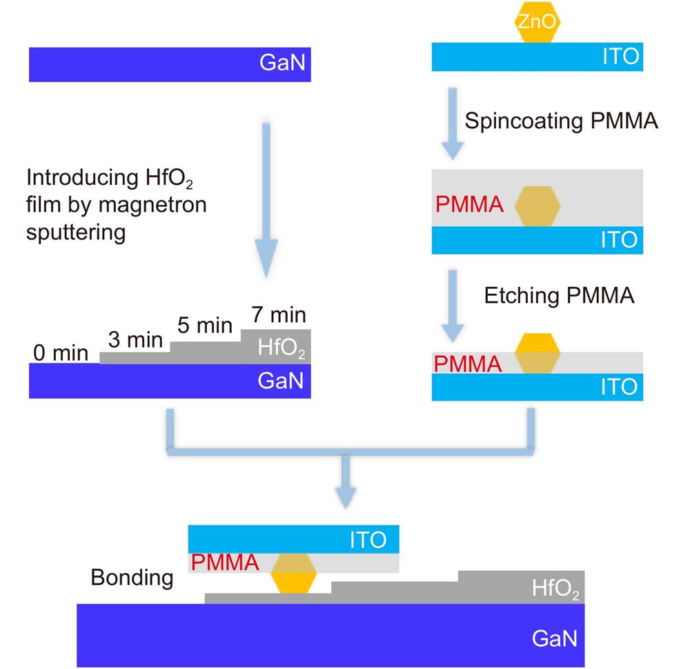
Fig. 1. The diagram of device fabrication.
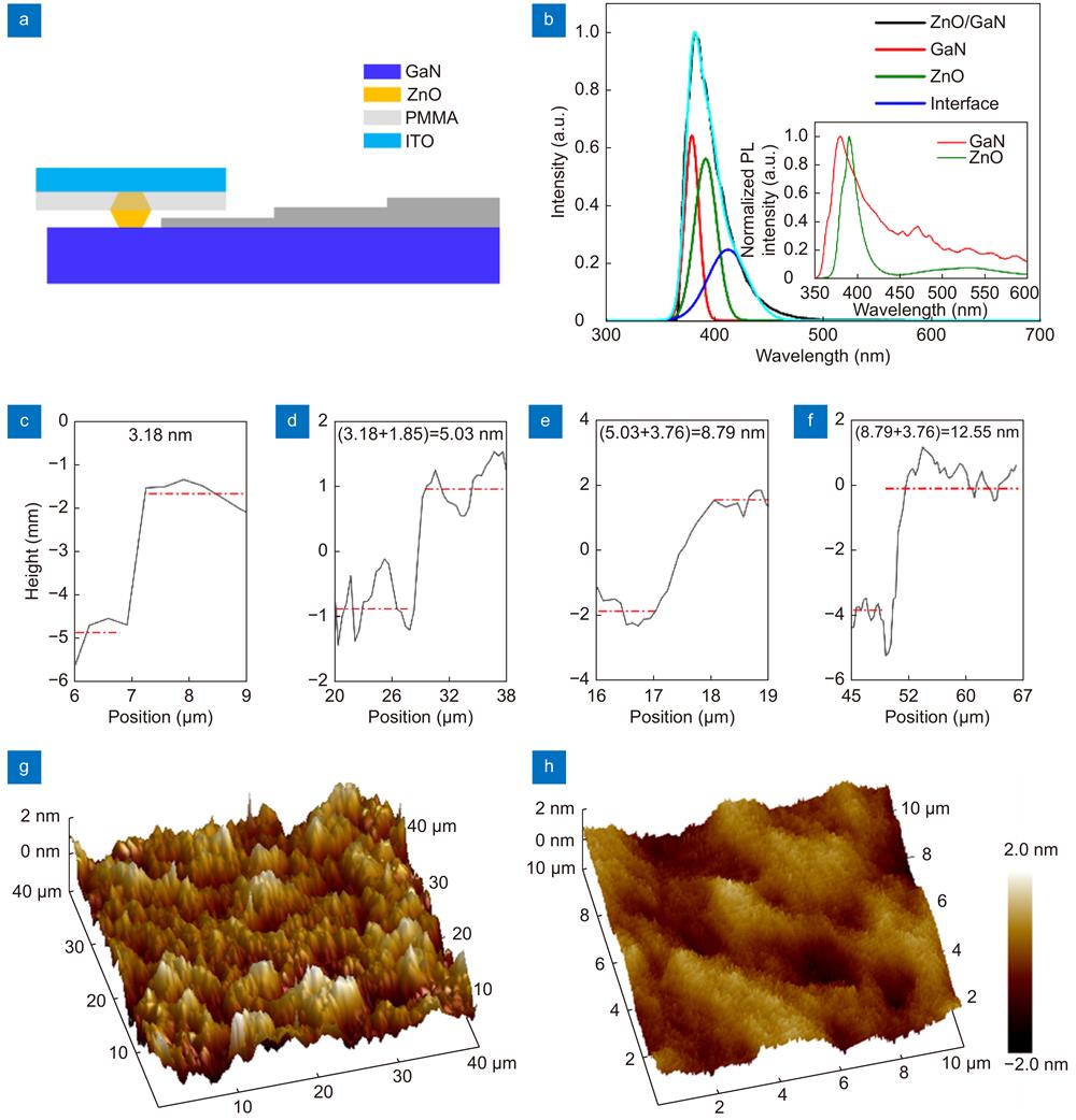
Fig. 2. (a ) A schematic diagram for ZnO/GaN LEDs. (b ) The Gaussian decomposition of EL spectra for LED and the inset depicts the PL spectra of the GaN film as well as ZnO MWs. (c−f ) The height of the step-like HfO2 film with different sputtering time (c) 2 min, (d) 3 min, (e) 5 min and (f) 7 min. (g , h ) AFM image for the GaN surface (g) before and (h) after bonding HfO2 film with thickness of 5.03 nm.
Fig. 3. (a ) Schematic diagram of ZnO/HfO2/GaN for in-situ optical test. (b ) Lasing emission intensity for ZnO MW versus the excitation power density on different substrates. (c −f ) the corresponding PL spectra under different excitation power densities for ZnO MW with different thickness of HfO2 films: (c) 0 nm, (d) 5.03 nm, (e) 8.79 nm and (f) 12.55 nm.
Fig. 4. The lifetime of ZnO MW on various substrates with excitation power of 8 μW .
Fig. 5. (a ) I-V characteristics of ITO/ZnO/HfO2/GaN LEDs. The inset is a schematic diagram for ITO/ZnO/HfO2/GaN LEDs. (b ) Normalized EL spectra for LEDs under an excitation current of 1 mA. (c−f ) EL intensity of ZnO/HfO2/GaN LEDs with HfO2 films of different thickness and the inset is the light pictures: (c) 0 nm, (d) 5.03 nm, (e) 8.79 nm, (f) 12.55 nm. (g ) Chromaticity coordinates of the spectra in (b). (h ) EL peak intensities of the LEDs from (c) to (f).
Fig. 6. Gaussian conversion of Fig. 5(c)−5(f) at a current of 1 mA : (a ) 0 nm, (b ) 5.03 nm, (c ) 8.79 nm, (d ) 12.55 nm, and the inset images depict the contents of UV and visible lights. (e ) The peak positions of emissions and (f ) FWHM of emissions for these LEDs.
Fig. 7. (a ) Energy band of ZnO/HfO2/GaN LEDs based on theoretical simulation. (b ) The distribution of electronical current density in ZnO/HfO2/GaN LEDs. The inset picture displays a structure diagram of simulation.
Fig. 8. Schematic band structures of (a ) ZnO/GaN, (b ) ZnO /thin HfO2/ GaN and (c ) ZnO /thick HfO2/ GaN.

Set citation alerts for the article
Please enter your email address
© Copyright 2018-2021 | Chinese Laser Press. All Rights Reserved 沪ICP备15018463号-20